January February 2022
Volume 26, Number 1
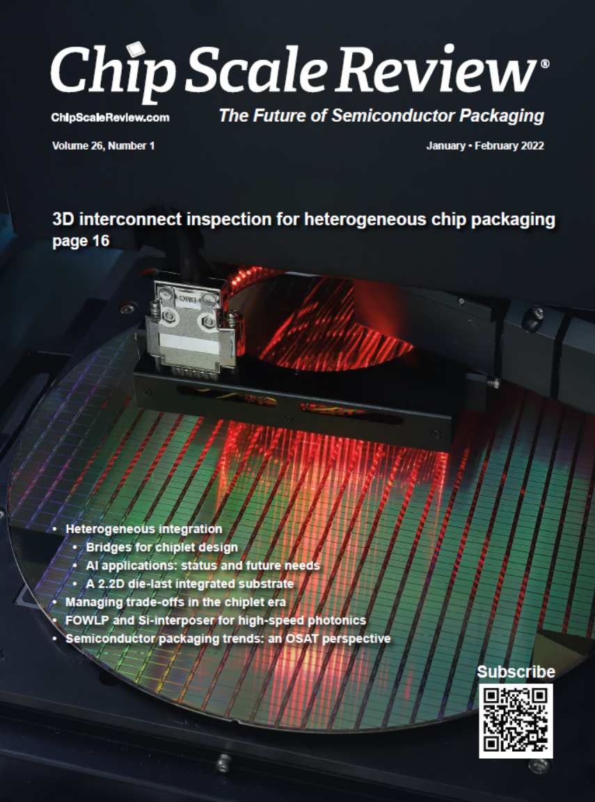
White-light scanning interferometry (WSI) applied for 100% fine-pitch interconnect inspection during wafer-level packaging. The WSI system includes scanning interferometry for large FOV, highspeed, and multi-reflectance surface 3D measurement. Interference patterns can be detected to calculate RDL dielectric layer thickness during panel/wafer-level 3D interconnect inspection.
Cover image courtesy of INTEKPLUS CO.,LTD.

March April 2022
Volume 26, Number 2
The chip shown in the picture is a fan-out multi-chip module (FO-MCM). It’s an example of heterogeneous integration fabrication with optimized 2/2μm line/spacing, multi-layers of redistribution layers (RDLs) and chip-last technology to supply interconnects between die to die and die to high-bandwidth memories. This becomes a potential platform for applications such as HPC, AI accelerator and cloud computing. Scalable routing capability makes this type of package competitive with respect to one using a conventional silicon interposer.
.
Cover image courtesy of SPIL

May June 2022
Volume 26, Number 3
Extending chiplet integration to 3D enables the placement of dies on top of each other, thereby providing added capacity without the added lateral distance. This keeps the latency low, and the ynamic power low. By freeing up valuable space inside the package, you can also fit more cores, and more transistors within a given package size.
Cover image courtesy of AMD

July August 2022
Volume 26, Number 4
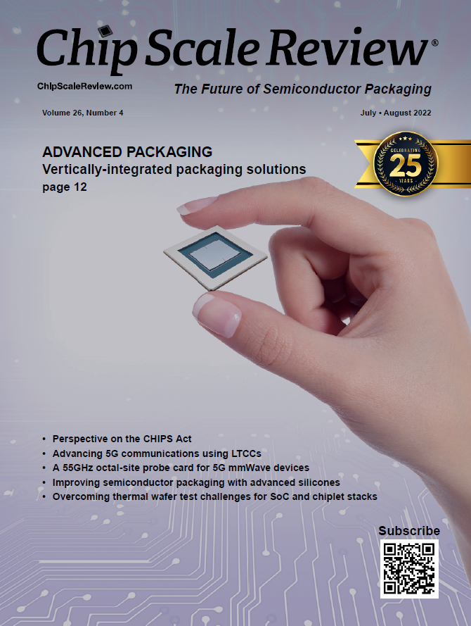
ASE’s advanced packaging is based on six critical packaging technologies. These technologies are built upon an open silicon ecosystem in partnership with foundries, component suppliers, and across the supply chain. Furthermore, these technologies provide the capabilities necessary to enable highly-integrated silicon packaging solutions.
.
Cover image courtesy of ASE, Inc.

September October 2022
Volume 26, Number 5
Challenges of direct hybrid bonding D2W remain in performance, yield and cost, which are driven by alignment capability, bonding quality and throughput, respectively.
.
Cover image copyright CEA-Leti, P. Jayet

November December 2022
Volume 26, Number 6
The cover article describes a doublesided probing system for 150μm-pitch copackaged optics (CPO). Such probing systems address the growing need for assured yield, particularly as heterogeneous integration is combined with silicon photonics needed for higher performance Ethernet applications to 800G.
.
Cover image courtesy of iStock/PhonlamaiPhoto


