previous arrow
CSR Issue Jan-Feb 2021
Chip Scale Review
January February 2021
Volume 25, Number 1

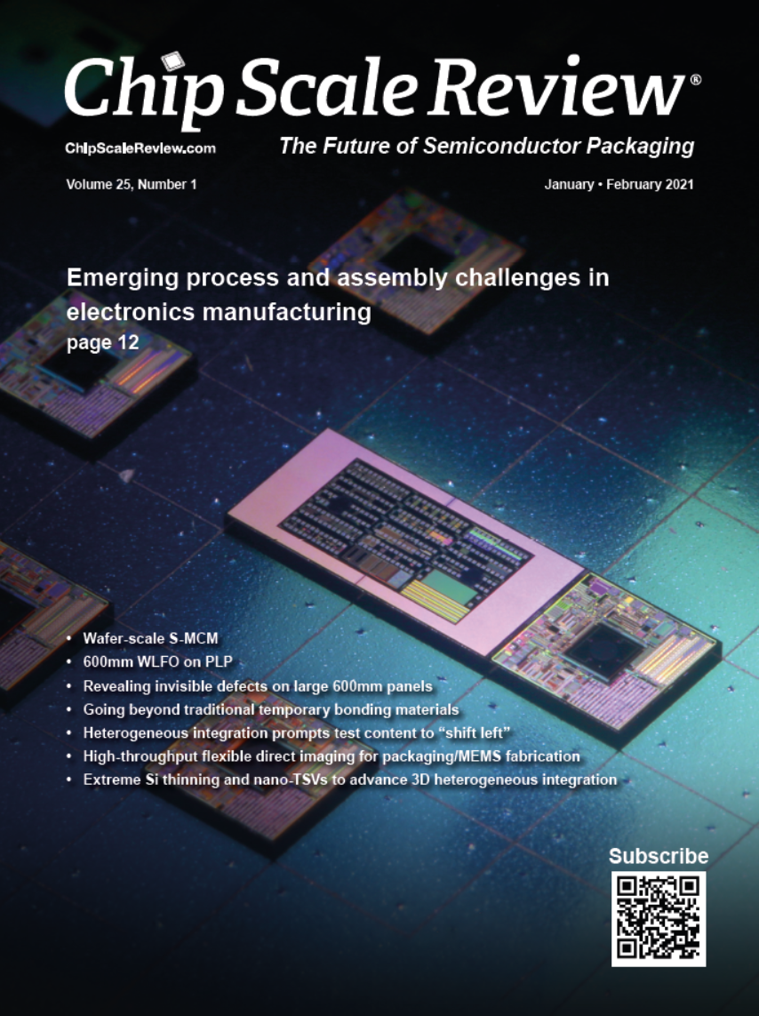
Cover image represents bare die on a wafer. These die were used in the assembly of a MEMS package, which was integrated into a pressure sensor. MEMS are responsible for the sensing element of heterogeneous integration and are one of many application types that will advance tremendously by leveraging intricate multi-die designs to deliver greater performance in a more compact footprint.

Photo courtesy of Universal Instruments

CSR March April 2021 Issue
Chip Scale Review
March April 2021
Volume 25, Number 2

CEA and IRT Nanoelec demonstrate a chiplet based Active Interposer proof-of-concept, IntAct. Using advanced 3D technologies, such as TSV-middle and fine-pitch die-to-die interconnect, the IntAct emonstrator exhibits state-of-the art performance. 150,000 die-to-die interconnects are used, mostly for power and grounds, while 30,000 μbumps are used for 3D plug connectivity delivering throughput density up to 3TBit/s/mm2. This circuit implements 96 cores with a scalable cache coherent architecture, delivering 220 GOPS peak.
.
Photo courtesy of CEA-Leti

CSR May June 2021 Issue
Chip Scale Review
May June 2021
Volume 25, Number 3

Microscopic image of a MEMSFlexâ„¢ high-density, tight-pitch MEMS probe array manufactured by Nidec SV TCL.
The MEMS probe card pictured has a multi-DUT layout and was fabricated with over 25,100 fully customized flat-tipped MEMS probes custom-designed for force, overdrive, length and tip style to meet the needs of a particular application
processor with small Cu pillars.
Photo courtesy of Nidec SV TCL

CSR July August 2021 Issue
Chip Scale Review
July August 2021
Volume 25, Number 4

Beyond Moore’s law, 3D semiconductors are the foundation for next-generation smart and connected devices. Hybrid bonding technologies enable 2.5D- and 3D-stacked integrated circuit (IC) solutions providing high-density chip-to-chip
connectivity to boost the computing performance in data center, gaming, artificial intelligence (AI), machine learning, autonomous vehicle, 5G and Internet of Things (IoT) applications.
.
Cover image courtesy of Xperi/Invensas

CSR September October 2021 Issue
Chip Scale Review
September October 2021
Volume 25, Number 5

The picture shows the result of a highly selective laser-assisted flip-chip removal from a randomly selected printed circuit board assembly. A ceramic tooling holds the chip after the separation step. A uniform and homogeneous solder depot matrix remains on the chip and board. The removed chip can be directly placed onto a new board to retain its functionality, or a new chip can be placed on the board.
.
Photo courtesy of PacTech – Packaging Technologies GmbH

CSR November December 2021 Issue
Chip Scale Review
November December 2021
Volume 25, Number 6

There are a plethora of devices and architectures that hold the promise of taking scaling beyond traditional Moore’s Law approaches. Research is being pursued in such technologies as qubits, spintronics, ultra-low power quantum devices, etc. But there is still much to be done with advancing transistor technologies, as well as the evolution of back-end-of-line technology. The cover article describes how graphene is being used to establish a new BEOL platform.
.
Cover image courtesy of Shutterstock

next arrow