Page 49 - Chip Scale Review_March-April_2024-digital
P. 49
growth occurring across the bonding
        interface. However,  there  are  some
        challenges of hybrid bonding  for
        HBM as pointed out by Micron [14]
        and are discussed below.
          P a r t i c l e s  g e ne r at e d  b y
        conventional wafer dicing.  Figure
        10 shows the particle counts before
        a nd af ter a laser stealt h dici ng,
        classifications of dicing particles,
        and signatures of particles. Micron
        fo u n d t h a t l a s e r s t e a lt h d ic i n g
        (Figure 10b) generated far more
        particles than that allowed by a Cu
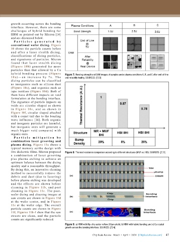
        hybr id  bondi ng  process  (Figure   Figure 7: Bonding strength and SAM images of samples under plasma conditions A, B, and C after end-of-line
        10 a) — a n  i n c r e a s e  b y  7 x .  T h e   and reliability testing. SOURCES: [7,13]
        dicing  particles  can  be  classified
        as inorganics such as silicon dust
        (Figure 10c), and organics such as
        tape residues (Figure 10d). Both of
        them have different impacts on void
        formulation at the bonding interface.
        The signature of particle impacts on
        voids are circular shaped as shown
        i n  Fig ure 10e, a nd a s show n i n
        Figure 10f, circular shaped attached
        with a comet tail due to the bonding
        wave inf luence [14]. Both organic
        and inorganic particles are harmful,
        but inorganic ones will generate a
        much bigger void compared with
        organic ones.
          P a r t i c l e m i t i g a t i o n b y
        combination  laser  grooving  and
        plasma dicing. Figure 11a shows a
        typical memory scribe design with
        five dielectric films. Micron proposed   Figure 8: Thermal resistance comparison according to different structures (MUF vs. HBI). SOURCES: [7,13]
        a combination of laser g rooving
        plus plasma etching to achieve an
        optimum balance between the dicing
        quality and a reasonable throughput.
        By doing this, an innovative cleaning
        method to successfully remove the
        debris and dust (due to lasering)
        before plasma etching was developed
        and the effects are  shown  before
        cleaning in  Figure  11b,  and post
        cleaning in  Figure 11c. The post-
        wafer dicing and cleaning images at
        saw streets are shown in Figure 11d
        at the wafer center, and in  Figure
        11e at the wafer edge. The overall
        particle counts are shown in Figure
        11f; Figures 11b-f show that the saw
        streets are clean, and the particle
        counts are significantly reduced.
                                           Figure 9: a) HBM with flip-chip solder reflow (20µm pitch); b) HBM with hybrid bonding; and c) Cu crystal
                                           growth across the bonding interface. SOURCES: [7,14]

                                                                                                             47
                                                             Chip Scale Review   March  •  April  •  2024   [ChipScaleReview.com]  47

