Page 46 - Chip Scale Review_March-April_2024-digital
P. 46

bonding surface of the core memory
                                                                              die after dicing and the buffer wafer.
                                                                              Plasma processing on the passivation
                                                                              surface creates an activation state and
                                                                              generates  the hydroxyl  group  (OH)
                                                                              when deionized (DI) water is sprayed
                                                                              onto the surface. Then, the chip is
                                                                              picked and aligned with the wafer
                                                                              (D2W), and the pressure applied for
                                                                              joining generates bindings among the
                                                                              oxides. These methods are repeated to
                                                                              stack several core memory dies as D2D
                                                                              layers. After pre-bonding is completed
                                                                              by stacking the layers, the bond
                                                                              between oxides is strengthened by high-
                                                                              temperature annealing; the Cu pads
                                                                              of the top and bottom plates expand
                                                                              and meet, electrically connecting as
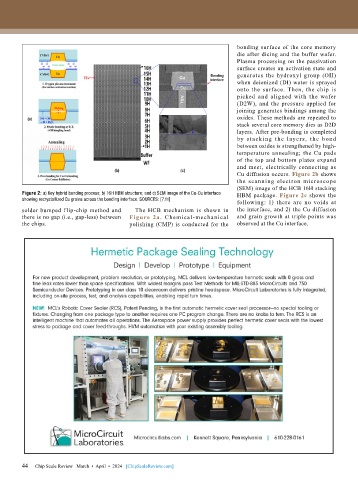
                                                                              Cu diffusion occurs. Figure 2b shows
                                                                              the scanning electron microscope
                                                                              (SEM) image of the HCB 16H stacking
        Figure 2: a) Key hybrid bonding process; b) 16H HBM structure; and c) SEM image of the Cu-Cu interface   HBM package. Figure 2c shows the
        showing recrystallized Cu grains across the bonding interface. SOURCES: [7,11]  following: 1) there are no voids at
        solder bumped flip-chip method and   The HCB mechanism is shown in    the interface, and 2) the Cu diffusion
        there is no gap (i.e., gap-less) between   Figure 2a. Chemical-mechanical   and grain growth at triple points was
        the chips.                         polishing (CMP) is conducted for the   observed at the Cu interface.


        44
        44   Chip Scale Review   March  •  April  •  2024   [ChipScaleReview.com]
   41   42   43   44   45   46   47   48   49   50   51