Page 43 - Chip Scale Review_March-April_2024-digital
P. 43
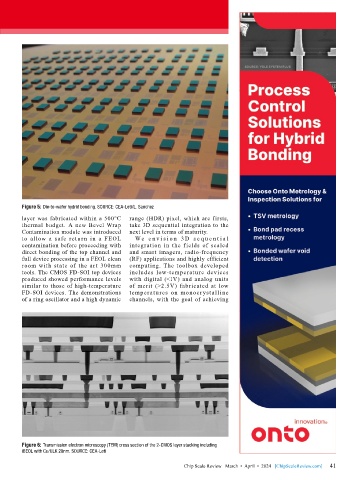
Figure 5: Die-to-wafer hydrid bonding. SOURCE: CEA-Leti/L. Sanchez
        layer was fabricated within a 500°C   range (HDR) pixel, which are firsts,
        thermal budget. A new Bevel Wrap   take 3D sequential integration to the
        Contamination module was introduced   next level in terms of maturity.
        to allow a safe retur n in a FEOL    We e n v i s i o n 3 D s e q u e n t i a l
        contamination before proceeding with   integration in the fields of scaled
        direct bonding of the top channel and   and smart imagers, radio-frequency
        full device processing in a FEOL clean   (RF) applications and highly efficient
        room with state of the art 300mm   computing. The toolbox developed
        tools. The CMOS FD-SOI top devices   includes low-temperature devices
        produced showed performance levels   with digital (<1V) and analog units
        similar to those of high-temperature   of merit (>2.5V) fabricated at low
        FD-SOI devices. The demonstrations   temperatures on monocr ystalline
        of a ring oscillator and a high dynamic   channels, with the goal of achieving


        Figure 6: Transmission electron microscopy (TEM) cross section of the 2-CMOS layer stacking including
        iBEOL with Cu/ULK 28nm. SOURCE: CEA-Leti

                                                                                                             41
                                                             Chip Scale Review   March  •  April  •  2024   [ChipScaleReview.com]  41

