Page 40 - Chip Scale Review_March-April_2024-digital
P. 40

TSV: A key enabling technology for
        heterogeneous systems
          In the framework of advanced dense
        interconnection, we have developed TSV
        processes since 2006, and consequently,
        we  have  the  requisite  experience  to
        contribute to the design of new modules
        or system architectures. We started
        with the TSV-last process for CMOS
        image sensor applications that are still
        being optimized for new computed
        tomography X-ray scanners or detectors
        for advanced particle physics needs.
        We then worked on TSV mid-process
        for memory on logic, and afterwards on
        silicon interposers application to more
        recent high-density (HD) TSV for logic
        blocks interconnections combined with
        hybrid density, for example.
          Each  of the  TSV  developments
        n ot e d  a b ove  fol lowe d  t h e  s a m e
        r i g o r o u s  p r o t o c ol ,  i n v ol v i n g
        o p t imi z a t i o n  o f  i t s  e l e c t r i c a l
        prop e r t ie s (re sist a nce, le a k age,
        capacitance) and qualif ication of
        reliabilit y nor ms — at f irst using
        passive test vehicle integration, and
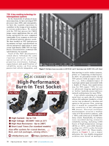
                                           Figure 1: Field higher beam cross section of a HD TSV (Ø=1µm H=10µm) daisy chain. SOURCE: CEA-Leti/R. Vélard
                                                                              then moving to active wafers (sensors,
                                                                              power or computing technologies).
                                                                              In 2023, we presented results on the
                                                                              TSV process with an aspect ratio of
                                                                              10:1, i.e., with a diameter/space of
                                                                              1μm/1μm (pitch 2μm) associated with
                                                                              a  depth  of  10μm;  this  application
                                                                              was for HD copper TSVs for use
                                                                              in advanced imaging applications
                                                                              or further backside power-delivery
                                                                              network architectures for nano TSVs.
                                                                                A test vehicle consisting of a single
                                                                              metal level on each side of a thinned
                                                                              silicon (Si) substrate bonded to a thick
                                                                              carrier was produced to develop and
                                                                              optimize the process flow, ensuring
                                                                              that it would be compatible with
                                                                              the constraints of the subsequent
                                                                              HB process. Electrical resistance
                                                                              measurements revealed a median
                                                                              value of 0.7Ω on Kelvin patterns, with
                                                                              a 100% yield achieved on 10,000-TSV
                                                                              daisy chains. Remarkably, no failures
                                                                              we re re corde d du r i ng ext e n sive
                                                                              reliability testing, including 2,000
                                                                              hours of high-temperature storage
                                                                              (HTS) at 150°C, and 2,000 thermal
                                                                              cycling test (TCT) cycles between
                                                                              -55°C and +150°C [8]. These results,
                                                                              show n i n  F ig ure 1, a re a major
                                                                              milestone for very highly-integrated
                                                                              architect ures based on multiple-


        38
        38   Chip Scale Review   March  •  April  •  2024   [ChipScaleReview.com]
   35   36   37   38   39   40   41   42   43   44   45