Page 45 - Chip Scale Review_March-April_2024-digital
P. 45
Cu-Cu hybrid bonding for high-bandwidth memory (HBM)


        By John H. Lau  [Unimicron Technology Corporation]
        H          y b r i d  b o n d i n g  h a s   by Yangtze Memory Technologies   mentioned in [2], Samsung has been


                   achieved quite a bit of
                                           NAND flash memory [1,2,7,8].
                                                                              its high-bandwidth memory (HBM)
                   t r a ct ion  re cently.  For   Company Ltd. (YMTC) on its 3D   in production for 3D-IC integration of
        example,  the 2023 IEEE Electronic   The brief fundamentals and recent   by f lip - ch ip h ig h-bondi ng force
        C o m p o n e n t s  a n d Te c h n o l o g y   a d v a n c e s a n d t r e n d s of C u - C u   thermocompression bonding (TCB)
        Conference (ECTC) featured more than   bumpless hybrid bonding from the   of the C2 (Cu-pillar with solder cap
        80 papers related to hybrid bonding.   IEEE/ECTC 2022 papers and IEEE/  or µbump) TSV (through-silicon via)
        In [1,2], it was mentioned that Cu-  ECTC 2023 papers have been reported,   chips with nonconductive film (NCF).
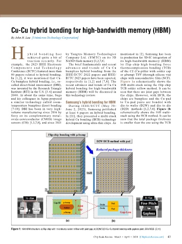
        Cu bumpless hybrid bonding, i.e., so-  respectively in [1,2] and [7,8]. The   Figure 1a schematically shows the
        called direct-bond interconnect (DBI),   recent advances and trends of Cu-Cu   16H  multi-stack  using the  flip-chip
        was invented by the Research Triangle   hybrid bonding for high-bandwidth   TCB solder reflow method. It can be
        Institute (RTI) in the U.S. [3-6] around   memory (HBM) will be discussed in   seen that there are joint gaps between
        2000. At about the same time, Suga   this technology review.          the chips. However, with HCB, the
        and his colleagues in Japan proposed                                  chips are bumpless and the Cu-pad
        a similar technology called room-  Samsung’s hybrid bonding for HBM   to Cu-pad pairs are bonded with
        temperature bumpless direct bonding   D u r i ng I EEE / EC TC ( M ay 30 -  die-to-wafer (D2W) and die-to-die
        [7-10]. DBI  has  been  in  very  high-  June  2, 2023),  Samsung  published   (D2D)  methods [1,2,7,8]. Figure 1b
        volume manufacturing since 2016 by   at least 6 papers on hybrid bonding.   schematically shows the 16H multi-
        Sony on its complementary metal-   In [11], they presented a multi-stack   stack using the HCB method. It can be
        oxide-semiconductor (CMOS) image   hybrid Cu bonding (HCB) technology   seen that the total package thickness
        sensors (CIS) [1,2,7,8], and since 2021   development using ultra-thin chips. As   is smaller than the one using the TCB


        Figure 1: 16H HBM structure: a) Flip chip with microbump solder reflow with joint gap; b) D2W/D2D Cu-Cu hybrid bonding with gapless joint. SOURCES: [7,11]

                                                                                                             43
                                                             Chip Scale Review   March  •  April  •  2024   [ChipScaleReview.com]  43

