Page 50 - Chip Scale Review_March-April_2024-digital
P. 50
IC integration packaging method.
                                                                                  3D NAND flash memory is a 3D
                                                                                  monolithic manufacturing method
                                                                                  within the chip. As mentioned in
                                                                                  [1,2], Yangtze Memory Technologies
                                                                                  Company Ltd. (YMTC) has been
                                                                                  manufacturing its 3D monolithic
                                                                                  NAND using the hybrid bonding
                                                                                  method within the chip (not the
                                                                                  package) since it licensed the Xperi
                                                                                  (now Adeia) Cu-Cu hybrid bonding
                                                                                  technology on October 12, 2021.
                                                                                •  Just like the 3D NAND, 3D DRAM is
                                                                                  a 3D monolithic chip manufacturing
                                                                                  method, which is a very hot topic
                                                                                  today. With respect to the research and
                                                                                  development results, such as patents (as
                                                                                  late as October 2022) on 3D monolithic
                                                                                  DRAMs, Micron (30) is leading
                                                                                  Samsung (15) and SK Hynix (10).
                                                                                  Recently, Samsung and SK Hynix have
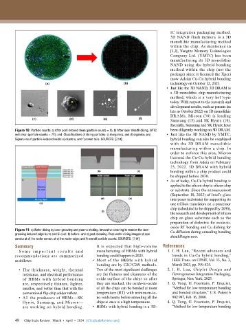
        Figure 10: Particle counts: a) After post-debond clean (particle counts = X); b) After laser stealth dicing, GPTC   been diligently working on 3D DRAM.
        wet clean (particle counts = 7X); and  Classifications of dicing particles: c) inorganics, and d) organics; and   •  Just like the 3D NAND by YMTC,
        Signatures of particle-induced voids: e) clusters, and f) comet tails. SOURCES: [7,14]  hybrid bonding can also be combined
                                                                                  with  the 3D  DRAM  monolithic
                                                                                  manufacturing within a chip. In
                                                                                  order to enforce this area, Micron
                                                                                  licensed the Cu-Cu hybrid bonding
                                                                                  technology from Adeia on February
                                                                                  23, 2022. 3D DRAM with hybrid
                                                                                  bonding within a chip product could
                                                                                  be shipped before 2030.
                                                                                •  As of today, Cu-Cu hybrid bonding is
                                                                                  applied to the silicon chip to silicon chip
                                                                                  or substrate. Since the announcement
                                                                                  (September 18, 2023) of Intel’s glass
                                                                                  interposer (substrate) for supporting its
                                                                                  one trillion transistors on a processor
                                                                                  chip (scheduled to be shipped by 2030),
                                                                                  the research and development of silicon
                                                                                  chip on glass substrate such as the
                                                                                  preparation of dielectric for oxide-to-
                                                                                  oxide RT bonding and Cu dishing for
        Figure 11: a) Wafer dicing by laser grooving and plasma etching. Innovative cleaning to remove the laser   Cu diffusion during annealing bonding
        grooving induced edge burrs and Si dust: b) before- and c) post-cleaning. Post-wafer dicing images at saw   should begin now.
        streets at d) the wafer center; at e) the wafer edge; and f) overall particle counts. SOURCES: [7,14]
        Summary                                It is expected that high-volume   References
          S o m e  i m p o r t a n t  r e s u l t s  a n d   manufacturing of HBMs with hybrid   1.  J. H. Lau, “Recent advances and
        recommendations are  summarized        bonding could happen in 2025.       trends in Cu-Cu hybrid bonding,”
        as follows:                          •  Most of the HBMs with hybrid       IEEE Trans. on CPMT, Vol. 13, No. 3,
                                               bonding are by C2C/C2W methods.     March 2023, pp. 399-425.
          •  The thickness, weight, thermal    Two of the most significant challenges   2.  J. H. Lau,  Chiplet  Design  and
            resistance, and electrical performance   are the flatness and cleanness of the   Heterogeneous Integration Packaging,
            of HBMs with hybrid bonding        oxide surface of the chips so after   Springer, New York, 2023.
            are, respectively thinner, lighter,   they are stacked, the oxide-to-oxide   3.  Q. Tong, G. Fountain, P. Enquist,
            smaller, and better than that with the   of all the chips can be bonded at room   “Method for low temperature bonding
            conventional flip-chip solder reflow.  temperature (RT) with minimum-to-  and bonded structure,” U.S. Patent 6
          •  All the producers of HBMs—SK      no voids/seams before annealing all the   902 987, Feb. 16, 2000.
            Hynix, Samsung, and Micron—        chips at once at a high temperature.  4.  Q. Tong, G. Fountain, P. Enquist,
            are working on hybrid bonding.   •  HBMs with hybrid bonding is a 3D-  “Method for low temperature bonding


        48   Chip Scale Review   March  •  April  •  2024   [ChipScaleReview.com]
        48

