Page 41 - Chip Scale Review_March-April_2024-digital
P. 41
layer wafer-to-wafer integrations.   integration, but the inclusion of a   TSV  integration  in  this  photonic
        Emerging data will be the subject of   2µm thick buried oxide (BOX) to   i nter poser was demonst rated by
        a forthcoming conference presenting   avoid parasitic coupling between   assessing the electrical yields and
        even  more  integrated  TSVs  landing   waveg u id e s a nd t he u nd e rly i ng   electro-optical performances of TSV
        on aggressively thinned metal 1, to   silicon was a real challenge. First, the   chains [10]. The f irst f unctional
        mimic the integration of 22nm or   TSV etching was fully redeveloped   inter mediate demonst rators have
        smaller nodes.                     to produce smooth sidewalls for later   just been assembled (Figure 3). This
                                           metallization and to eliminate the   st udy contributes to the ongoing
        Active interposers: Enhancing      silicon etching below the BOX; then,   prog ress i n comput i ng system s,
        photonic and HPC applications      the thermomechanical deformation   particularly in the realm of HPC,
          From an architectural point of view,   of t he t h i n subst r ate due to t he   by providing insights and solutions
        our interest in interposers started in   thick BOX had to be compensated   to integrate optical communication
        2010 with the development of large   by  balancing  all  the  between-layer   technologies within a heterogeneous
        passive interposers [9]. Since then, this   st resses li n ked  to  f ront side  a nd   computing architecture.
        theme has followed its own roadmap   backside i nter poser i nteg rat ion.   By c o mbi n i ng 3D i nt eg r a t io n
        alongside developments in advanced   These adjustments were mandatory   w i t h m i d - p r o c e s s T S V a n d
        HPC, requiring increased bandwidth,   for the assembly of the top dies of   a d va n c e d p a c k a g i ng , b a s e d o n
        reduced latency and greater power   t he Popst a r photon ic i nter poser   small-pitch f lip ch ips a nd opt ic
        efficiency. From passive interposers,   demonstrator (Figure 2) hosting four   f ib er pig t a i l i ng, he ter oge ne ou s
        the technology has moved to active   computation chiplets and six electro-  integration  of a photonic  device on
        i nter poser s i nclud i ng act ive 3D   optical driver chips. The successful   a silicon interposer was achieved.
        links and embedded DC-DC (direct                                      T h i s  r e p r e s e n t s  t h e f u n c t i o n a l
        current) converters for pinpoint power                                demonstration of the next generation
        delivery. It has finally matured for                                  of beam steering for a light detection
        use in photonic interposers, making it                                a n d r a n g i n g ( Li DA R) d e sig n e d
        possible to overcome the latency wall                                 for autonomous vehicle d r ivi ng.
        that emerges with increasing chip-                                    Figure 4 shows integration of the
        to-chip distances even with these on-                                 f lip chip in an optical phase array
        chip architectures. For each of these                                 (OPA) generating the laser beam
        approaches, dedicated technological                                   scanning a silicon interposer, thanks
        developments were required, starting                                  t o  a  10µm  TSV  a nd  40µm  pit ch
        f r o m  p a s s i v e i n t e r p o s e r s w i t h
        integration of the first 10µm diameter
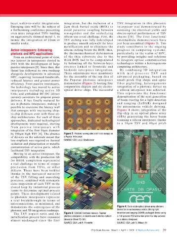
        by 100µm high TSV [6]. The absence   Figure 2: Photonic waveguides and micro bumps on
        of devices on the substrate meant that   a Popstar Interposer.
        less emphasis was required on thermal   SOURCE: CEA-Leti/J. Charbonnier
        oxidation and planarization or metallic
        contamination of active parts, which
        facilitated TSV integration.
          Moving to an active interposer, the
        compatibility with the production fab
        for BEOL completion represented
        a real challenge in terms of copper
        prot r u sion f rom  TSVs ,  or ot he r
        defects. These have been tackled
        thanks to the increased maturity
        of the TSV f illing and annealing
        processes, combined with systematic
        close inspection of each TSV in the
        closed loop by industrial process
        teams to determine optimal process
        points. These  developments related
        to photonic inter posers represent
        a real brea k t h roug h i n ter ms of
        interconnections, as mentioned, and
        demonstrate the convergence of the                                    Figure 4: Solid-state optical phase array photonic
        photonic and 3D integration roadmaps.                                 device for an autonomous vehicle driving light
          T he  TSV a sp e ct  r at io a nd t he   Figure 3: STARAC frontside module: Popstar   detection and ranging (LiDAR) packaged device using
        metallization process have remained   photonic interposer, 4 chiplets and 6 electro-optical   a mid-process TSV and a fine-pitch flip-chip process
        almost unchanged since the f irst   drivers in 28nm FD-SOI.           on a silicon interposer.
                                           SOURCE: CEA-Leti/R. Franiatte      SOURCE: CEA-Leti/ N. Miloud-Ali

                                                                                                             39
                                                             Chip Scale Review   March  •  April  •  2024   [ChipScaleReview.com]  39

