Page 35 - Chip Scale Review_March-April_2024-digital
P. 35
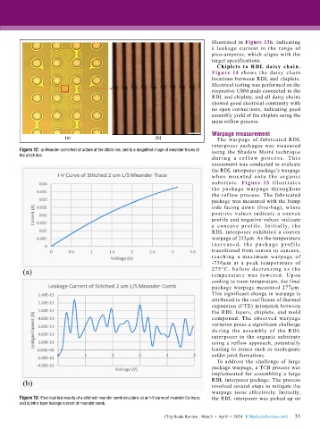
illustrated in Figure 13b, indicating
                                                                              a leakage current in the range of
                                                                              pico-amperes, which aligns with the
                                                                              target specifications.
                                                                                Chiplets to R DL daisy chain.
                                                                              Figure 14 shows the daisy chain
                                                                              locations between RDL and chiplets.
                                                                              Electrical testing was performed on the
                                                                              respective UBM pads connected to the
                                                                              RDL and chiplets; and all daisy chains
                                                                              showed good electrical continuity with
                                                                              no open connections, indicating good
                                                                              assembly yield of the chiplets using the
                                                                              mass reflow process.

                                                                              Warpage measurement
                                                                                The warpage of fabricated RDL
                                                                              interposer packages was measured
        Figure 12: a) Meander comb test structure at the stitch line; and b) a magnified image of meander traces at   using the Shadow Moiré technique
        the stitch line.
                                                                              d u r i ng a r e f l o w p r o c e s s . T h i s
                                                                              assessment was conducted to evaluate
                                                                              the RDL interposer package’s warpage
                                                                              whe n mou nt e d ont o t he orga n ic
                                                                              subst r at e.  F ig ure 15 illu st r ates
                                                                              the package war page th roughout
                                                                              the ref low process. The fabricated
                                                                              package was measured with the bump
                                                                              side facing down (live-bug), where
                                                                              positive values indicate a convex
                                                                              profile and negative values indicate
                                                                              a concave prof ile. I n it ially, t he
                                                                              RDL interposer exhibited a convex
                                                                              warpage of 213µm. As the temperature
                                                                              i n c r e a s e d , t h e p a c k a g e p r of i l e
                                                                              transitioned from convex to concave,
                                                                              reaching a maximum war page of
                                                                              -736µm at a peak temperature of
                                                                              275°C, before decreasi ng as t he
                                                                              tempe r at u re  wa s  lowe red.  Upon
                                                                              cooling to room temperature, the final
                                                                              package warpage measured 277µm.
                                                                              This significant change in warpage is
                                                                              attributed to the coefficient of thermal
                                                                              expansion (CTE) mismatch between
                                                                              the RDL layers, chiplets, and mold
                                                                              compound. The observed warpage
                                                                              variation poses a significant challenge
                                                                              du r ing the assembly of the R DL
                                                                              interposer to  the organic  substrate
                                                                              using a reflow approach, potentially
                                                                              leading to issues such as inadequate
                                                                              solder joint formations.
                                                                                To  address  the  challenge  of  large
                                                                              package warpage, a TCB process was
                                                                              implemented for assembling a large
                                                                              RDL interposer package. The process
                                                                              involved several steps to mitigate the
                                                                              warpage issue effectively. Initially,
        Figure 13: Electrical test results of a stitched meander comb structure: a) an I-V curve of meander Cu trace;   the RDL interposer was picked up on
        and b) intra-layer leakage current of meander comb.

                                                                                                             33
                                                             Chip Scale Review   March  •  April  •  2024   [ChipScaleReview.com]  33

