Page 32 - Chip Scale Review_March-April_2024-digital
P. 32
a semi-additive process (SAP). The   organic substrate. Underfill material   tool and was subjected to a heating
        photolithography stepper used in   was dispensed and cured to bridge the   profile mimicking actual solder
        this work  has a  maximum  exposure   solder bump gap between the RDL     reflow conditions. The Shadow
        field size of 44 × 26.7mm, and two-  interposer and the organic substrate.  Moi ré optical tech nique was
        field  mask  stitching  was  utilized  to   Te st i ng.  T h e f a b r ic a t e d R DL   employed to accurately measure
        create the large package size of 52 ×   interposers were subjected to electrical   the warpage of the RDL interposer
        44mm.  Figure 4 displays the wafer   and warpage measurement as follows:   under controlled conditions.
        map during photomask exposure. The
        wafer map during photomask exposure   1.  Meander combs with 2µm L/   Results and discussion
        was illustrated in Figure 4. Chiplets   S positioned at the stitched area   The following sections discuss RDL
        with micro-bump interconnects were     between the 2 mask f ields to   interposer fabrication results: 1) Cu
        assembled onto the top under bump      verify the continuity of the of the   RDL process results, and 2) the chiplet
        metallization (UBM) pads on the RDL    two RDL traces. A daisy chain   assembly wafer-level molding and
        stacks using a mass reflow process.    connecting the chiplets to the RDL   RDL interposer package assembly.
        Wa fe r-level e p ox y c om p r e s sio n   layers was utilized to confirm the   Cu RDL process results.  Figure
        molding was applied to encapsulate     continuity of the solder bumps and    5a shows the RDL and UBM layers
        the chiplets and RDL stacks with an    RDL interposer.                fabricated on a temporary transparent
        expoxy molding compound, forming     2. Warpage measurement is crucial   carrier, prior to chiplets assembly.
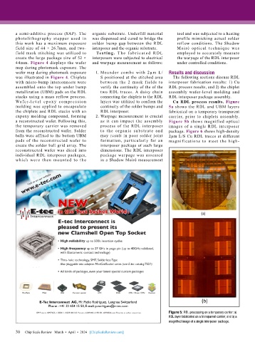
        a reconstructed wafer. Following this,   as  it  can  impact  the  assembly   Figure 5b shows magnified optical
        the temporary carrier was removed      process of the RDL interposer   images of a single RDL interposer
        from the reconstructed wafer. Solder   to the organ ic subst rate and   package. Figure 6 shows high-density
        balls were affixed to the bottom UBM   may result in poor solder joint   2µm L/S Cu RDL traces at different
        pads of the reconstructed wafer to     formation, particularly for an   magnif ications to meet the high-
        create the solder ball grid array. The   interposer package of such large
        reconstructed wafer was diced into     dimensions. The RDL interposer
        individual RDL interposer packages,    package  warpage  was  assessed
        which were then mou nted to the        in a Shadow Moiré measurement


                   E-Tec Interconnect  AG, Mr. Pablo Rodriguez,  Lengnau Switzerland
                       Phone : +41 32 654 15 50, E-mail: p.rodriguez@e-tec.com
                                                                              Figure 5: RDL processing on a temporary carrier: a)
                                                                              RDL layer fabricated on a transparent carrier; and b) a
                                                                              magnified image of a single interposer package.

        30
        30   Chip Scale Review   March  •  April  •  2024   [ChipScaleReview.com]

