Page 34 - Chip Scale Review_March-April_2024-digital
P. 34
Meander comb test structure at   whe r e t he t wo t r a ce s c onve rge.
                                           the stitch line.  Figure 12 shows a   Additionally,  Figure 13a  presents
                                           2µm line/space meander comb test   the I-V curve of the meander trace,
                                           structure positioned at the stitch line   demonstrating good connectivity for
                                           between the two masks in the field. A   the stitched Cu traces. The measured
                                           slight taper is visible at the junction   i n t r a - l a y e r l e a k a g e c u r r e n t i s


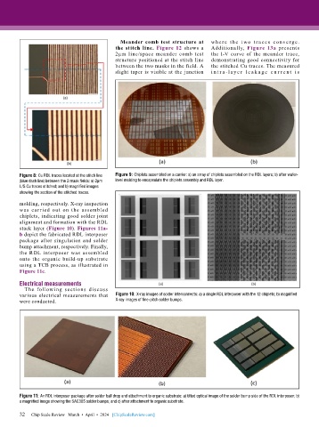
        Figure 8: Cu RDL traces located at the stitch line   Figure 9: Chiplets assembled on a carrier: a) an array of chiplets assembled on the RDL layers; b) after wafer-
        (blue dash line) between the 2 mask fields: a) 2µm   level molding to encapsulate the chiplets assembly and RDL layer.
        L/S Cu traces stitched; and b) magnified images
        showing the section of the stitched traces.
        molding, respectively. X-ray inspection
        was carried out on the assembled
        chiplets, indicating good solder joint
        alignment and formation with the RDL
        stack layer (Figure 10). Figures 11a-
        b depict the fabricated RDL interposer
        package after singulation and solder
        bump attachment, respectively. Finally,
        the RDL interposer was assembled
        onto the organic build-up substrate
        using a TCB process, as illustrated in
        Figure 11c.

        Electrical measurements
          The following sections discuss
        various electrical measurements that   Figure 10: X-ray images of solder interconnects: a) a single RDL interposer with the 12 chiplets; b) magnified
        were conducted.                    X-ray images of fine-pitch solder bumps.


        Figure 11: An RDL interposer package after solder ball drop and attachment to organic substrate: a) tilted optical image of the solder bump side of the RDL interposer; b)
        a magnified image showing the SAC305 solder bumps; and c) after attachment to organic substrate.

        32   Chip Scale Review   March  •  April  •  2024   [ChipScaleReview.com]
        32

