Page 33 - Chip Scale Review_March-April_2024-digital
P. 33
bandwidth requirement of the chiplets.   the Cu traces was observed along the
                                           Figure 7a shows the 3µm diameter   stitching line boundary. The stepper
                                           contact  via  openings  patterned  in  a   tool mask align ment accuracy is
                                           photodielectric  film  for  connecting   maintained to below 0.2µm to ensure
                                           the different level of Cu RDL, while   good stitching between the mask field.
                                           Figure 7b shows the landing pads and   Chiplet assembly, wafer-level
                                           Cu traces processed over the contact   m o l d i n g a n d R D L  i n t e r p o s e r
                                           vias.  Figure 8 shows the fine-pitch   package assembly.  Figures 9a-b
                                           Cu traces fabricated at the stitching   show the optical images of the chiplets
                                           section (blue dash line) between the   assembled onto the RDL stack on the
                                           two mask fields. No discontinuity in   carrier wafer and after wafer-level


                                                 BALL PLACEMENT & LASER SOLDERING


                                                  3D-Soldering  Solder Stacking  Wire Soldering  BGA Soldering


        Figure 6: A segment of the high-density 2µm L/S Cu
        RDL traces at different magnifications.

                                                  Pre-Soldering of  Lid Sealing for  Flex to Chip  Through Hole
                                                  SMD Connector  Connectors &  Soldering   Soldering
                                                    Elements     IR-Sensors

                                                 LASER ASSISTED BONDING (LAB, LCB, LAR)


                                                   3D Multi Layer  Optoelectronic  CPU on Interposer  SMD Capacitor
                                                  Stacked Packaging  Device Assembly  Assembly  Assembly
                                                 SOLDER & CHIP REPAIR


                                                     BGA       Interconnects of  BGA Package Assembly  Flex to Flex
                                                     Rework     Camera Module  onto Substrate  Seperation


                                                         WE MANUFACTURE

                                                           EQUIPMENT FOR

                                                                YOUR NEEDS


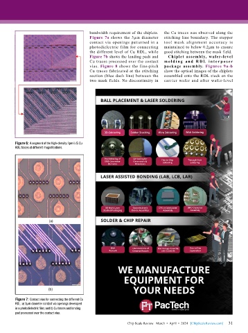
        Figure 7: Contact vias for connecting the different Cu
        RDL: a) 3µm diameter contact via openings developed
        in a photodielectric film; and b) Cu traces and landing
        pad processed over the contact vias.

                                                                                                             31
                                                             Chip Scale Review   March  •  April  •  2024   [ChipScaleReview.com]  31

