Page 30 - Chip Scale Review_March-April_2024-digital
P. 30
Using an RDL-first FOWLP process to develop a large


        RDL interposer package


        By Soon Wee Ho, Siew Boon Soh, Boon Long Lau, Hsiao Hsiang-Yao, Vempati Srinivasa Rao
        [Institute of Microelectronics, A*STAR (Agency for Science, Technology and Research)]
        T        h e c h i p l e t s p a c k a g i ng   designs.  While SoC  technology has   A m o n g  t h e  d i f fe r e nt  ch iple t s


                 approach has emerged as
                                           h i g h - p e r f or m a nc e   a p p l i c a t i on
                                                                              first or chip-last FOWLP [6] approach
                 a promisi ng alter native   historically been utilized to construct   packaging approaches, the R DL-
        to system on chip (SoC) technology,   systems by i nteg r at i ng mult iple   has emerged as a novel and effective
        offering a low-cost and faster-to-  technologies and functional blocks   paradigm  for  fabricating  chiplets
        market  solution  for  building  high-  onto a monolithic chip, the growing   packages. This methodology prioritizes
        performance application systems.   complexity of SoC designs has led to   the fabrication of high-density RDL
        This work presents a redistribution   longer development times and higher   layers on a temporary carrier substrate,
        layer (R DL)-f irst fan-out wafer-  manufacturing costs. In contrast,   allowing for the efficient processing of
        level packaging (FOWLP) fabrication   chiplets offer a modular and scalable   multiple RDL layers with minimal wafer
        process for creating a large organic   approach that enables companies to   warpage. By adopting the RDL-first
        R D L i n t e r p o s e r f o r c h i p l e t s   build systems by combining chips from   approach, semiconductor companies
        packaging. The process involves    diverse technologies using advanced   can  integrate  chiplets  with  micro-
        assembling chiplets with micro -   packaging platforms.               bumps, create sophisticated chiplets
        bumps onto a high-densit y f ine-    Var ious platfor ms for chiplets   systems, and develop large organic RDL
        pitch RDL stack, encapsulating them   packaging have been developed,   interposers with embedded chiplets.
        with mold compound, and creating   each offering unique advantages and   This approach  not only enhances
        a reconstr ucted wafer. Electrical   challenges. These platforms include   performance and cost-efficiency but also
        and war page measurements were     embedding chiplets in a FOWLP based   streamlines the assembly process and
        conducted to assess the performance   on an RDL interposer technology   ensures the continuity of RDL traces
        of the fabricated RDL interposer.   [1,2], assembling chiplets on silicon   across the entire package area.
        Results show successful fabrication   interposers [3,4], or utilizing high-  I n t h is work , a n orga n ic R DL
        of the R DL inter poser with good   density build-up organic substrates   interposer with a large package size
        electrical continuity and solder joint   [5]. The choice of platform depends   of 52 x 44mm, housing 12 embedded
        formation, despite challenges related   on fa ct or s such a s p e r for m a nce   chiplets on a 60 x 60mm organic
        to warpage during assembly. A thermal   requirements, cost considerations,   substrate was developed, showcased
        compression bonding (TCB) process   and scalability needs, with the RDL   the effectiveness of the RDL-first
        was implemented to address warpage   technology serving as a critical enabler   FOWLP process in realizing complex
        is s ue s , de mon st r at i ng ef fe c t ive   for all chiplets systems. The demand for   chiplets systems.
        assembly of the R DL i nter poser   high-density RDL layers to facilitate
        onto an organic substrate. This work   routing between multiple chiplet I/Os   Experimental procedure
        highlights the potential of the RDL-  poses challenges such as large package   The following sections address process
        first FOWLP process for large chiplets   areas and the need for precise mask   flow and testing considerations.
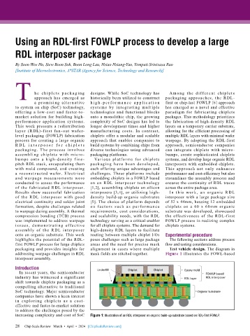
        packaging and provides insights for   alignment in cases where multiple   Test vehicle design. The diagram in
        addressing warpage challenges in RDL   mask fields are stitched together.  Figure 1 illustrates the FOWL-based
        interposer assembly.

        Introduction
          In recent years, the semiconductor
        industry has witnessed a significant
        shift towards chiplets packaging as a
        compelling alternative to traditional
        SoC technology. Major semiconductor
        companies have shown a keen interest
        i n explor i ng ch iplet s a s a cost-
        effective and faster-to-market solution
        to address the challenges posed by the
        increasing complexity and cost of SoC   Figure 1: Illustration of an RDL interposer on organic build-up substrate based on RDL-first FOWLP.

        28   Chip Scale Review   March  •  April  •  2024   [ChipScaleReview.com]
        28

