Page 25 - Chip Scale Review_March-April_2024-digital
P. 25
key optical component functions, such as   the PIC overhang design allows sufficient
        accommodating the signal conversion and   space to assemble optical fiber.
        processing to gain bandwidth/speed and   Application of the FO-EB process
        lower power consumption. Furthermore,   for an OE. The process flow of FO-EB


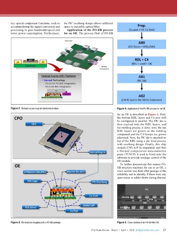
        Figure 2: OE build-up as a signal conversion module.                  Figure 4: Application of the FO-EB process for an OE.
                                                                              for an OE is described in Figure 4. First,
                                                                              the bottom RDL layers and Cu post will
                                                                              be configured in parallel. The EIC die is
                                                                              then stacked onto the RDL layers, and
                                                                              the molding process is done; next, the top
                                                                              RDL layers are grown on the molding
                                                                              compound and the C4 bumps are grown
                                                                              afterward. Next, the PIC die is attached on
                                                                              top of the RDL using a die bond process
                                                                              with overhang design. Finally, this chip
                                                                              module (CM) will be singulated; and then
                                                                              a thermal compression nonconductive
                                                                              paste (TCNCP) is used to bond onto the
                                                                              substrate to provide warpage control of the
                                                                              OE module.
                                                                                To further demonstrate this mature FO-
                                                                              EB structure readiness for use in an OE, a
                                                                              cross section was done after passage of the
                                                                              reliability test to identify if there were any
                                                                              open traces or solder shorts during thermal


        Figure 3: OE structure mapping with a FO-EB package.                  Figure 5: Cross section of an FO-EB-like OE.

                                                                                                             23
                                                             Chip Scale Review   March  •  April  •  2024   [ChipScaleReview.com]  23

