Page 20 - Chip Scale Review_March-April_2024-digital
P. 20
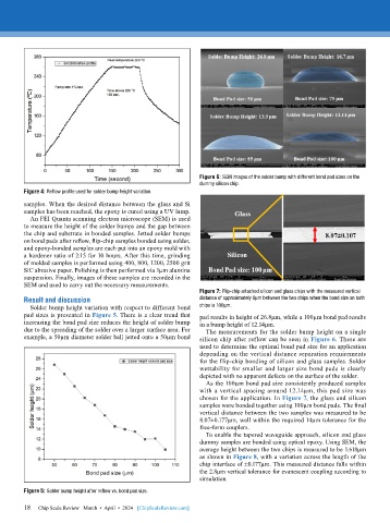
Figure 6: SEM images of the solder bump with different bond pad sizes on the
                                                             dummy silicon chip.
        Figure 4: Reflow profile used for solder bump height variation.
        samples. When the desired distance between the glass and Si
        samples has been reached, the epoxy is cured using a UV lamp.
          An FEI Quanta scanning electron microscope (SEM) is used
        to measure the height of the solder bumps and the gap between
        the chip and substrate in bonded samples. Jetted solder bumps
        on bond pads after reflow, flip-chip samples bonded using solder,
        and epoxy-bonded samples are each put into an epoxy mold with
        a hardener ratio of 2:15 for 10 hours. After this time, grinding
        of molded samples is performed using 400, 800, 1200, 2500 grit
        SiC abrasive paper. Polishing is then performed via 1µm alumina
        suspension. Finally, images of these samples are recorded in the
        SEM and used to carry out the necessary measurements.
                                                             Figure 7: Flip-chip attached silicon and glass chips with the measured vertical
        Result and discussion                                distance of approximately 8µm between the two chips when the bond size on both
          Solder bump height variation with respect to different bond   chips is 100µm.
        pad sizes is presented in Figure 5. There is a clear trend that   pad results in height of 26.8µm, while a 100µm bond pad results
        increasing the bond pad size reduces the height of solder bump   in a bump height of 12.14µm.
        due to the spreading of the solder over a larger surface area. For   The measurements for the solder bump height on a single
        example, a 50µm diameter solder ball jetted onto a 50µm bond   silicon chip after reflow can be seen in Figure 6. These are
                                                             used to determine the optimal bond pad size for an application
                                                             depending on the vertical distance separation requirements
                                                             for the flip-chip bonding of silicon and glass samples. Solder
                                                             wettability for smaller and larger size bond pads is clearly
                                                             depicted with no apparent defects on the surface of the solder.
                                                               As the 100µm bond pad size consistently produced samples
                                                             with a vertical spacing around 12.14µm, this pad size was
                                                             chosen for the application. In Figure 7, the glass and silicon
                                                             samples were bonded together using 100µm bond pads. The final
                                                             vertical distance between the two samples was measured to be
                                                             8.07±0.177µm, well within the required 14µm tolerance for the
                                                             free-form couplers.
                                                               To enable the tapered waveguide approach, silicon and glass
                                                             dummy samples are bonded using optical epoxy. Using SEM, the
                                                             average height between the two chips is measured to be 1.618µm
                                                             as shown in Figure 8, with a variation across the length of the
                                                             chip interface of ±0.177µm. This measured distance falls within
                                                             the 2.8µm vertical tolerance for evanescent coupling according to
                                                             simulation.
        Figure 5: Solder bump height after reflow vs. bond pad size.

        18   Chip Scale Review   March  •  April  •  2024   [ChipScaleReview.com]
        18

