Page 23 - Chip Scale Review_March-April_2024-digital
P. 23
A package solution for an optical engine in


        silicon photonics


        By David Ho, Steven Lin, YP. Wang  [Siliconware Precision Industries Co., Ltd]
        D          ata center traffic is growing   technology to integrate the electrical   and optimal integration of electronics


                   at a compound annual growth
                   rate of nearly 30% because   integrated chip (EIC) and the photonics   chips and photonics chips, the length
                                                                              of electrical links can be significantly
                                           integrated chip (PIC) next to graphics
        of the substantial growth of 5G, Internet   processing  units  (GPUs)  and  router   shortened. Therefore, the interconnect
        of Things (IoT), artificial intelligence   switches. Driven by artificial intelligence   bandwidth density and energy efficiency
        (AI) and high-performance computing   (AI)  applications,  silicon  photonics   can be much improved.
        (HPC) applications. Over the next two   technology will become a key technology   With the development of router/
        generations the switching throughput   in the semiconductor industry.  switch devices, with the bandwidth at
        jumps from 12.8Tb/s to 25.6Tb/s,  and                                 1.8T, the link speed of copper wire can
        51.2Tb/s over the next two generations.   Introduction                still provide a matching transmission
        The number of transceivers per switch   As silicon scaling comes closer to the   efficiency. However, with the evolution
        and the data rates of those transceivers   limits of physics, future reduction of the   of  application-specific  integrated
        will increase as well. Scaling density will   gate oxide does not decrease the cost   circuits (ASICs) and the addition of high
        favor smaller connectors and lower power   per transistor. The demand for higher   bandwidth memory (HBM) die—when
        consumption. Additionally, in order to meet   functionality and lower cost of electronic   the bandwidth is increased to more than
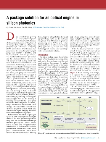
        the tremendous bandwidth requirements   devices, however, will not be coming to   10Tbps—an optical module needs to be
        derived from transmitting large amounts   an end. To improve yield and lower the   used to provide a 200Gbps to 400Gbps
        of data, optical communication technology   total cost, the semiconductor industry is   transmission channel as shown in
        has made great progress because the   breaking down a large die to chiplet-based   Figure 1. When reaching over 25Tbps,
        growth rate of conventional pluggable   devices. Chiplet packaging, therefore,   it is expected that the pluggable optical
        optical components is not able to catch up   becomes a key technology to continue   module will be transformed into an
        with the growth rate of data center traffic.   Moore’s Law. The multiple chiplet   integrated silicon light engine to shorten
        Furthermore, traditional copper wire is   packages can be horizontally/vertically   the communication distance between
        limited by bandwidth, distance and power   stacked on a Si interposer using through-  the ASIC die and the optical engine to
        requirements. In parallel, the optical   silicon via (TSV) technology (2.5D) or on   achieve a transmission speed >400G.
        package is developing from wire bond, to   an organic interposer to build up a fan-out   A CPO application is different from
        flip chip and wire bond as a hybrid package,   multi-chip module (FOMCM) or a fan-  traditional pluggable optical transceiver
        and then moving to 3DIC or fan-out   out embedded bridge (FO-EB). Through   module technologies. A CPO application
        technology to support optical engine (OE)   such advanced packaging technologies   combines a silicon photonic chip, a
        development. Silicon photonics, therefore,
        is becoming a promising technology to
        replace copper wire and the industry is
        becoming convinced that it is a good option
        to transmit data with greater bandwidth,
        longer transmission distance and better
        energy efficiency than conventional
        electrical integrated circuits, which may
        suffer serious signal integrity distortion
        when transmitting data at high speed.
          In this article, the critical co-packaged
        optics (CPO) concept was brought
        out to be the next-generation platform
        along with the fan-out embedded bridge
        (FO-EB) package as a robust option
        for an OE solution, to approach the
        enhancement of optical interconnection
        performance, broader bandwidth, lower
        power consumption and smaller form
        factor. CPO utilizes vertical 3D stacking   Figure 1: Trends in data center switches and transceivers. SOURCE: Yole Développement, Silicon Photonics, 2020

                                                                                                             21
                                                             Chip Scale Review   March  •  April  •  2024   [ChipScaleReview.com]  21

