Page 21 - Chip Scale Review_March-April_2024-digital
P. 21
3.  L. Brusberg, et al., “Glass substrate
                                                                                   with integrated waveguides for
                                                                                   surface mount photonic packaging,”
                                                                                   Jour. of Lightwave Tech., vol. 39, no. 4,
                                                                                   pp. 912-919, 15 Feb.15, 2021.
                                                                                 4.  L. Ranno, et al., “Integration of
                                                                                   free-form micro-optics with PICs
                                                                                   for sensing, packaging, and optical
                                                                                   manipulation,” Frontiers in Optics
                                                                                   + Laser Science 2022 (FIO, LS),
                                                                                   Technical Digest Series (Optica Pub.
                                                                                   Group, 2022).
                                                                                 5.  S. Yu, et al., “Free-form micro-optical
                                                                                   reflectors for broadband and low-loss
                                                                                   fiber-to-chip coupling,” Conference on
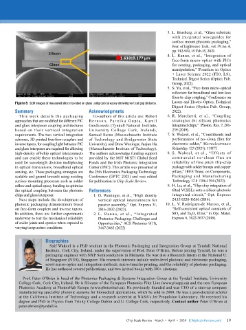
        Figure 8: SEM images of measured silicon bonded on glass using optical epoxy showing vertical gap distance.  Lasers and Electro-Optics, Technical
                                                                                   Digest Series (Optica Pub. Group,
        Summary                            Acknowledgments                         2022).
          This work details the packaging    Co-authors of this article are: Robert   6.  R. Marchetti, et al., “Coupling
        approaches that are modified for different PIC   Be r n son , Pa r n i k a G upt a , K a m il   strategies for silicon photonics
        and glass interposer coupling architectures   Gradkowski (Tyndall National Institute,   integrated chips,”  Photon. Res. 7, 201-
        based on their vertical integration   University  College  Cork,  Ireland),   239 (2019).
        requirements. The two vertical integration   Samuel Serna (Massachusetts Institute   7.  S. Wakeel, et al., “Constituents and
        schemes, 3D printed free-form couplers and   of Technology and Bridgewater State   performance of no-clean flux for
        inverse tapers, for coupling light between PIC   University), and Drew Weninger, Juejun Hu   electronic solder,” Microelectronics
        and glass interposer are required for allowing   (Massachusetts Institute of Technology).   Reliability 123 (2021): 114177.
        high-density off-chip optical interconnects   The authors acknowledge funding support   8.  S. Wakeel, et al., “Effects of
        and can enable these technologies to be   provided by the MIT MISTI Global Seed   commercial  no-clean  f lux  on
        used for wavelength division multiplexing   Funds and the Irish Photonic Integration   reliability of fine pitch flip-chip
        in optical transceivers, broadband optical   Center (IPIC). This article was presented at   package with solder bumps and copper
        sensing, etc. These packaging strategies are   the 25th Electronics Packaging Technology   pillars,” IEEE Trans. on Components,
        scalable and geared towards using existing   Conference (EPTC 2023) and was edited   Packaging and Manufacturing
        surface mounting processes such as solder   for publication in Chip Scale Review.  Technology 12.8 1386-1394 (2022).
        reflow and optical epoxy bonding to optimize                             9.  H. Lu, et al., “Flip-chip integration of
        the optical coupling between the photonic   References                     tilted VCSELs onto a silicon photonic
        chips and glass interposer.           1.  D. Weninger, et al., “High density   integrated circuit,” Opt. Express
          Next steps include the development of   vertical optical interconnects for   24.1516258-16266 (2016).
        photonic packaging demonstrators based   passive assembly,” Opt. Express 31,   10.  L. V. Rodríguez-de Marcos, et al.,
        on free-form couplers and inverse tapers.   2816-2832 (2023).              “Self-consistent optical constants of
        In addition, there are further experiments   2.  L. Ranno, et al., “Integrated   SiO 2  and Ta 2 O 5  films,” in Opt. Mater.
        underway to test the mechanical reliability   Photonics Packaging: Challenges and   Express 6, 3622-3637 (2016).
        of solder joints and epoxies when exposed to   Opportunities,” ACS Photonics 9(11),
        varying temperature conditions.         3467-3485 (2022)


                       Biographies
                         Saif Wakeel is a PhD student in the Photonic Packaging and Integration Group at Tyndall National
                       Institute, Cork City, Ireland, under the supervision of Prof. Peter O’Brien. Before joining Tyndall, he was a
                       packaging engineer with NXP Semiconductors in Malaysia. He was also a Research Intern at the National U.
                       of Singapore (NUS), Singapore. His research interests include wafer-level photonic and electronic packaging,
                       novel micro-optics and integration methods, micro-transfer printing, and the reliability of photonic packaging.
                       He has authored several publications, and two invited books with 380+ citations.

            Prof. Peter O’Brien is head of the Photonics Packaging & Systems Integration Group at the Tyndall Institute, University
          College Cork, Cork City, Ireland. He is Director of the European Photonics Pilot Line (www.pixapp.eu) and the new European
          Photonics Academy at PhotonHub Europe (www.photonhub.eu). He previously founded and was CEO of a start-up company
          manufacturing speciality photonic systems for biomedical applications, which he sold in 2009. He was a post-doctoral scholar
          at the California Institute of Technology and a research scientist at NASA’s Jet Propulsion Laboratory. He received his
          degree and PhD in Physics from Trinity College Dublin and U. College Cork, respectively. Contact author Peter O’Brien at
          peter.obrien@tyndall.ie


                                                                                                             19
                                                             Chip Scale Review   March  •  April  •  2024   [ChipScaleReview.com]  19

