Page 19 - Chip Scale Review_March-April_2024-digital
P. 19
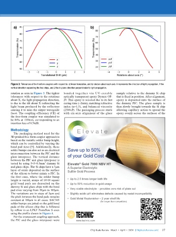
Figure 3: Tolerances of the freeform couplers with respect to: a) linear translation, and b) rotation about each axis. X represents the direction of light propagation, Y the
        vertical direction separating the two chips, and Z the in-plane direction perpendicular to light propagation.
        rotation as seen in Figure 3. The tighter   bonded together via U V- cu rable   sample relative to the dummy Si chip
        tolerances with respect to the rotations   optically transparent epoxy Dymax OP-  that is fixed in position. After alignment,
        about X, the light propagation direction,   29. This epoxy is selected due to its fast   epoxy is deposited onto the surface of
        is due to the tilt about X redirecting the   curing time (~2min), matching refractive   the dummy PIC. The glass sample is
        light beam produced by the reflectors   index (n=1.5), and balanced viscosity   then slowly brought towards the Si chip
        causing it to miss the output waveguide   (2500cP). The packaging process starts   allowing capillary action to spread the
        facet. The coupling efficiency (CE) of   with six-axis alignment of the glass   epoxy evenly across the surfaces of the
        the free-form coupler was simulated to
        be 84% at 1550nm, corresponding to an
        insertion loss of 0.76dB.

        Methodology
          The packaging method used for the
        3D-printed free-form coupler approach is
        based on the variable solder bump height,
        which can be controlled by varying the
        bond pad sizes [9]. Additionally, these
        solder bumps can also act as an electrical   Save up to 50%
        interconnection between the PIC and the
        glass interposer. The vertical distance   of your Gold Cost
        between the PIC and glass interposer is
                               3
        tested by using 5×5×0.5mm  dummy Si   Elevate  Gold 7990 NBV HT
                                                      ®
        and glass chips. The Si chips have a 3µm   A Superior Electrolytic
        layer of oxide deposited on the surface   Sulfite Gold Process
        of the silicon to better mimic a PIC. In
        the first case, where the solder bump
        height is varied, arrays of 14×14 square   •  Up to 2.5 times longer bath life
        gold bond pads are deposited on the   •  Up to 50% reduction in gold usage
        dummy Si and glass chips with the bond
        pad sizes varying from 50µm to 105µm.   •  Very stable electrolyte – provides zero risk of plate out
        The variations are in steps of 5µm and   •  Slightly acidic pH eliminates defects caused by resist incompatibility
        the pitch between the bond pads remains
        constant at 100µm in all cases. SAC305   •  Gold Metal Replenisher – 2 year shelf life
                                                                    (8x longer than competitors)
        solder bumps are jetted on the gold bond
        pads of the silicon chip that is followed
        by reflow in an LPKF Protoflow S oven
        using the profile shown in Figure 4.
          For the evanescent coupling approach,
        the PIC and the glass interposer were       www.technic.com


                                             Chip Scale Review - Elevate Gold NBV HT 2023 - Gold savings.indd   1  3/6/2024   3:56:50 PM
                                                                                                   3/6/2024   3:56:50 PM
                                             Chip Scale Review - Elevate Gold NBV HT 2023 - Gold savings.indd   1
                                                                                                             17
                                                             Chip Scale Review   March  •  April  •  2024   [ChipScaleReview.com]  17

