Page 14 - Chip Scale Review_March-April_2024-digital
P. 14
We report here results from the first two steps, namely ALoT
                                                             bonding and LT wafer thinning.
                                                               Figure 6 shows an ALoT-bonded LT-glass wafer. Due to
                                                             imperfect cleaning, voids are seen inside the wafer as well as
                                                             near the edge. The edge voids would cause delamination during
                                                             thinning, so careful trimming was applied to make sure these
                                                             are removed. When necessary, the trimming wheel performed
                                                             linear, “surgical” actions to ensure the edge voids were removed.
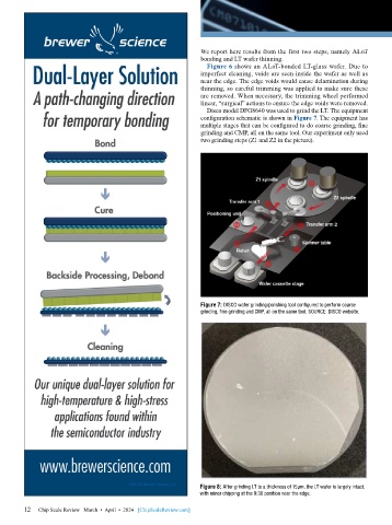
                                                               Disco model DFG8640 was used to grind the LT. The equipment
                                                             configuration schematic is shown in Figure 7. The equipment has
                                                             multiple stages that can be configured to do coarse grinding, fine
                                                             grinding and CMP, all on the same tool. Our experiment only used
                                                             two grinding steps (Z1 and Z2 in the picture).


                                                             Figure 7: DISCO wafer grinding/polishing tool configured to perform coarse
                                                             grinding, fine grinding and CMP, all on the same tool. SOURCE: DISCO website.


                                                             Figure 8: After grinding LT to a thickness of 15µm, the LT wafer is largely intact,
                                                             with minor chipping at the 9:30 position near the edge.

        12   Chip Scale Review   March  •  April  •  2024   [ChipScaleReview.com]
        12

