Page 9 - Chip Scale Review_March-April_2024-digital
P. 9
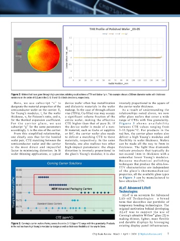
Figure 2: Wafers that have gone through high-precision polishing could achieve a TTV well below 1µm. This example shows a 300mm diameter wafer with thickness
        variations on the order of 0.2µm in the 3, 6, 9 and 12 o’clock directions, respectively.
          He re, we u se subsc r ipt “s” t o   device wafer often has metallization   inversely proportional to the square of
        designate the material properties of the   and dielectric materials in the wafer   the carrier wafer thickness.
        semiconductor wafer on the carrier: E s    makeup. In the case of through-silicon   As a result of understanding the
        for Young’s modulus, t s  for the wafer   vias (TSVs), Cu-filled vias may occupy   relationships noted above, we now
        thickness, υ s  for Poisson’s ratio, and α s    a significant volume fraction of the   offer glass wafers that cover a wide
        for the thermal expansion coefficient.   entire wafer, making the effective   range of CTEs with fine granularity.
        F o r t h e  c a r r i e r g l a s s , w e u s e   CTE higher than that of pure Si. If   F i g u r e 3  sho w s a v a i l a b i l i t y
        subscript “g” for the same parameters   the device wafer is made of a non-  between CTE values ranging from
        accordingly. L is the size of the carrier.  Si material, such as GaAs or sapphire   3-12.5ppm/°C. For products in the
          From this simplified relationship,   or SiC, the carrier wafer also needs   red box, the carrier glass wafers also
        one clearly sees that for the bonded   to  deliver  a matching  CTE  to  these   deliver a high Young’s modulus and
        wafer pair, CTE matching between the   materials, respectively. In the same   flexibility in wafer thickness. Wafers
        semiconductor wafer and the carrier   formula, one also realizes two other   can be made all the way to 5mm in
        is the most direct and impactf ul   high-impact parameters: the shape   thickness. The light blue diamonds
        factor in minimizing distortion. In Si   distortion is inversely proportional to   indicate products that typically do
        wafer thinning applications, a typical   the glass’s Young’s modulus; it is also   not exceed 1mm in thickness with a
                                                                              somewhat lower Young’s modulus.
                                                                              B e c a u s e  m e c h a n i c a l  p o l i sh i n g
                                                                              techniques that produce the ultra-low-
                                                                              TTV characteristics are independent
                                                                              of the glass’s ther momechanical
                                                                              properties, all the available glass types
                                                                              in Figure 3 can be manufactured to
                                                                              have ultra-low-TTV.
                                                                              ALoT: Advanced Liftoff
                                                                              Technologies
                                                                                ALoT is an acronym for Advanced
                                                                              Li f t- of f Te ch nolog ie s — a b r o a d
                                                                              term that describes our portfolio of
                                                                              temporary bonding technologies. The
                                                                              original motivation behind developing
                                                                              A LoT was to suppor t the use of
                                                                              Corning’s ultrathin Willow  glass [2] in
                                                                                                    ®
                                                                              making thinner, lighter, more flexible
                                                                              and durable displays by leveraging
        Figure 3: Corning’s carrier wafer offering covers the entire 3-12.6ppm/°C range with fine granularity. Products
        in the red box have high Young’s modulus by design as well as thickness flexibility all the way to 5mm.  existing display panel infrastructure.
                                                             Chip Scale Review   March  •  April  •  2024   [ChipScaleReview.com]  7 7

