Page 8 - Chip Scale Review_March-April_2024-digital
P. 8
High-precision wafer thinning using ultra-low-TTV


        glass carrier and temporary bonding


        By Jay Zhang  [Corning Incorporated]
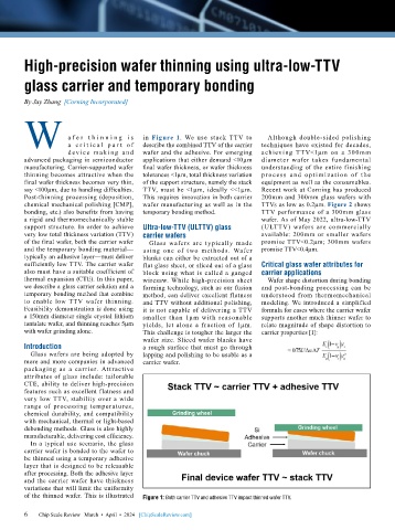
        W            a f e r t h i n n i n g i s   in  Figure 1. We use stack TTV to   Although double-sided polishing


                     a  c r i t i c a l  p a r t  o f
                     d ev ic e m a k i ng a nd   describe the combined TTV of the carrier   techniques have existed for decades,
                                                                              achieving TTV<1µm on a 300mm
                                           wafer and the adhesive. For emerging
        advanced packaging in semiconductor   applications that either demand <10µm   diameter wafer takes fundamental
        manufacturing. Carrier-supported wafer   final wafer thickness, or wafer thickness   understanding of the entire finishing
        thinning becomes attractive when the   tolerances <1µm, total thickness variation   process  a nd  opt i m i zat ion  of  t he
        final wafer thickness becomes very thin,   of the support structure, namely the stack   equipment as well as the consumables.
        say <100µm, due to handling difficulties.   TTV, must be <1µm, ideally <<1µm.   Recent work at Corning has produced
        Post-thinning processing (deposition,   This requires innovation in both carrier   200mm and 300mm glass wafers with
        chemical mechanical polishing [CMP],   wafer manufacturing as well as in the   TTVs as low as 0.2µm. Figure 2 shows
        bonding, etc.) also benefits from having   temporary bonding method.  TTV performance of a 300mm glass
        a rigid and thermomechanically stable                                 wafer. As of May 2022, ultra-low-TTV
        support structure. In order to achieve   Ultra-low-TTV (ULTTV) glass   (ULTTV) wafers are commercially
        very low total thickness variation (TTV)   carrier wafers             available: 200mm or smaller wafers
        of the final wafer, both the carrier wafer   Glass  wafers are  typically  made   promise TTV<0.2µm; 300mm wafers
        and the temporary bonding material—  using one of two methods. Wafer   promise TTV<0.4µm.
        typically an adhesive layer—must deliver   blanks can either be extracted out of a
        sufficiently low TTV. The carrier wafer   flat glass sheet, or sliced out of a glass   Critical glass wafer attributes for
        also must have a suitable coefficient of   block using what is called a ganged   carrier applications
        thermal expansion (CTE). In this paper,   wiresaw. While high-precision sheet   Wafer shape distortion during bonding
        we describe a glass carrier solution and a   forming technology, such as our fusion   and post-bonding processing can be
        temporary bonding method that combine   method, can deliver excellent flatness   understood from thermomechanical
        to enable low TTV wafer thinning.   and TTV without additional polishing,   modeling. We introduced a simplified
        Feasibility demonstration is done using   it is not capable of delivering a TTV   formula for cases where the carrier wafer
        a 150mm diameter single crystal lithium   smaller than 1µm with reasonable   supports another much thinner wafer to
        tantalate wafer, and thinning reaches 5µm   yields, let alone a fraction of 1µm.   relate magnitude of shape distortion to
        with wafer grinding alone.         This challenge is tougher the larger the   carrier properties [1]:
                                           wafer size. Sliced wafer blanks have
        Introduction                       a rough surface that must go through
          Glass wafers are being adopted by   lapping and polishing to be usable as a
        more and more companies in advanced   carrier wafer.
        packaging as a carrier. Attractive
        attributes of glass include: tailorable
        CTE, ability to deliver high-precision
        features such as excellent flatness and
        very low TTV, stability over a wide
        range of processing temperatures,
        chemical durability, and compatibility
        with mechanical, thermal or light-based
        debonding methods. Glass is also highly
        manufacturable, delivering cost efficiency.
          In a typical use scenario, the glass
        carrier wafer is bonded to the wafer to
        be thinned using a temporary adhesive
        layer that is designed to be releasable
        after processing. Both the adhesive layer
        and the carrier wafer have thickness
        variations that will limit the uniformity
        of the thinned wafer. This is illustrated   Figure 1: Both carrier TTV and adhesive TTV impact thinned wafer TTV.

        6 6  Chip Scale Review   March  •  April  •  2024   [ChipScaleReview.com]

