Page 10 - Chip Scale Review_March-April_2024-digital
P. 10
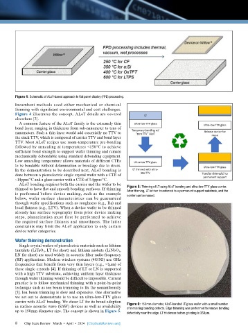
Figure 4: Schematic of ALoT-based approach to flat panel display (FPD) processing.
        Incumbent methods used either mechanical or chemical
        thinning with significant environmental and cost challenges.
        Figure 4 illustrates the concept. ALoT details are covered
        elsewhere [3].
          A common feature of the ALoT family is the extremely thin
        bond layer, ranging in thickness from sub-nanometer to tens of
        nanometers. Such a thin layer would add essentially no TTV to
        the stack TTV, which is composed of carrier TTV and bond layer
        TTV. Most ALoT recipes use room-temperature pre-bonding
        followed by annealing at temperatures <150°C to achieve
        sufficient bond strength to support wafer thinning and remain
        mechanically debondable using standard debonding equipment.
        Low annealing temperature allows materials of different CTEs
        to be bondable without delamination or breakage due to stress.
        In the demonstration to be described next, ALoT bonding is
        done between a piezoelectric single crystal wafer with a CTE of
        ~14ppm/°C and a glass carrier with a CTE of 3.4ppm/°C.
          ALoT bonding requires both the carrier and the wafer to be
        thinned to have flat and smooth bonding surfaces. If thinning   Figure 5: Thinning of LT using ALoT bonding and ultra-low-TTV glass carrier.
        is performed before device making, such as the example   After thinning, LT is then transferred to a permanent support substrate, and the
        below, wafer surface characteristics can be guaranteed   carrier can be reused.
        through wafer specifications such as roughness (e.g., Ra) and
        local flatness (e.g., LTV). When a device wafer to be thinned
        already has surface topography from prior device making
        steps, planarization must first be performed to achieve
        the required surface flatness and smoothness. The latter
        constraints may limit the ALoT application to only certain
        device wafer categories.

        Wafer thinning demonstration
          Single crystal wafers of piezoelectric materials such as lithium
        tantalate (LiTaO 3 , LT for short) and lithium niobate (LiNbO 3 ,
        LN for short) are used widely in acoustic filter radio-frequency
        (RF) applications. Modern wireless systems (4G/5G) use GHz
        frequencies that benefit from very thin layers (e.g., <1µm) of
        these single crystals [4]. If thinning of LT or LN is supported
        with a high TTV substrate, achieving uniform layer thickness
        through wafer thinning would be difficult to impossible. Current
        practice is to follow mechanical thinning with a point-by-point
        technique such as ion beam trimming to fix the nonuniformity
        [5]. Ion beam trimming is slow and expensive. One alternative
        we set out to demonstrate is to use an ultra-low-TTV glass
        carrier with ALoT bonding. We chose LT for its broad adoption
        in surface acoustic wave (SAW) devices as well as availability   Figure 6: 150mm diameter, ALoT-bonded LT/glass wafer with a small number
        up to 150mm diameter size. The concept is shown in Figure 5.   of remaining bonding defects. Edge trimming was performed to remove bonding
                                                             defectivity near the edge. LT thickness before grinding is 350µm.
        8 8  Chip Scale Review   March  •  April  •  2024   [ChipScaleReview.com]

