Page 15 - Chip Scale Review_March-April_2024-digital
P. 15
acoustic microscopy (CSAM). The standard mitigation method is to
                                                             introduce edge trimming around the entire wafer before bonding.
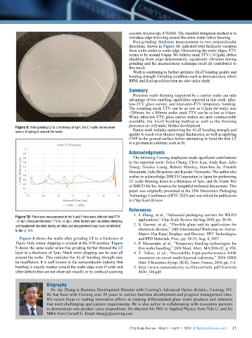
                                                               Post-grinding thickness measurement in two perpendicular
                                                             directions, shown in Figure 10, indicated total thickness variation
                                                             from wafer center to wafer edge. Discounting the wafer edges, TTV
                                                             seems to be around 0.4µm. We believe stack TTV (~0.2µm), debris
                                                             shedding from edge delamination, equipment vibration during
                                                             grinding and the measurement technique itself all contributed to
                                                             this result.
                                                               Work is continuing to further optimize ALoT bonding quality and
                                                             bonding strength. Grinding conditions such as down pressure, wheel
                                                             RPM, and feed speed/direction are also under study.

                                                             Summary
                                                               Precision wafer thinning supported by a carrier wafer can take
                                                             advantage of two enabling capabilities reported in this work: ultra-
                                                             low-TTV glass carrier, and near-zero-TTV temporary bonding.
                                                             The resulting stack TTV can be as low as 0.2µm for wafer size
                                                             <200mm; for a 300mm wafer, stack TTV can be as low as 0.4µm.
                                                             While ultra-low-TTV glass carrier wafers are now commercially
                                                             available, the ALoT bonding method as well as the thinning
        Figure 9: After grinding LT to a thickness of 5µm, the LT wafer shows more   processes are still under further development.
                                                               Future work includes optimizing the ALoT bonding strength and
        severe chipping all around the wafer.
                                                             quality to reach even thinner target thicknesses, as well as applying
                                                             CMP to the ground surface before attempting to bond the thin LT
                                                             to a permanent substrate such as Si.
                                                             Acknowledgments
                                                               The following Corning employees made significant contributions
                                                             to the reported work: Erica Chang, Chris Kuo, Andy Kuo, Julie
                                                             Tseng, Gwako Liang, Robert Manley, Han-hee Jo, Prantik
                                                             Mazumder, Julia Brueckner and Kuniaki Yamazaki. The author also
                                                             wishes to acknowledge DISCO Corporation in Japan for performing
                                                             LT wafer thinning down to a thickness of 5µm, and Dr. Frank Wei
                                                             of DISCO Hi-Tec America for insightful technical discussions. This
                                                             paper was originally presented at the 25th Electronics Packaging
                                                             Technology Conference (EPTC 2023) and was edited for publication
                                                             in Chip Scale Review.

                                                             References
                                                               1.  J. Zhang, et al., “Advanced packaging carriers for WLFO
        Figure 10: Thickness measurement in the X and Y directions indicate total TTV
        ~0.4µm. Because the stack TTV is ~0.2µm, other factors such as debris shedding,   applications,” Chip Scale Review Jul/Aug 2019, pp. 20-26.
        and equipment vibration during grinding and measurement may have contributed   2.  S. Garner, et al., “Flexible glass and its application for
        to the LT TTV.                                           electronic devices,” 24th International Workshop on Active-
                                                                 Matrix Flat Panel Displays and Devices: TFT Technologies
          Figure 8 shows the wafer after grinding LT to a thickness of   and FPD Materials, Proc., pp. 28-33, Aug. 8, 2017.
        15µm. Only minor chipping is evident at the 9:30 position. Figure   3.  P. Mazumder, et al., “Temporary bonding technologies for
        9 shows the same wafer when fine grinding further thinned the LT   thin wafer handling,” 2018 Meet. Abstr. MA2018-02, p. 950.
        layer to a thickness of 5µm. Much more chipping can be seen all   4.  T. Takai, et al., “Incredible high-performance SAW
        around the wafer. This indicates the ALoT bonding strength may   resonator on novel multi-layered substrate,” 2016 IEEE
        be insufficient. It is well known in the semiconductor industry that   Inter. Ultrasonics Symp. (IUS), Tours, France, 2016, pp. 1-4.
        bonding is usually weaker around the wafer edge even if voids and   5.  http://www.nanoindustry.su/files/article pdf/4/article
        other defectivities are not observed visually or by confocal scanning   4630_330.pdf


                       Biography
                         Dr. Jay Zhang is Business Development Director with Corning’s Advanced Optics division, Corning, NY.
                       He has been with Corning over 20 years in various business development and program management roles.
                       His recent focus is leading innovation efforts at creating differentiated glass wafer products and solutions
                       that meet challenging applications requirements. He is also active in collaborating with ecosystem partners
                       to demonstrate new product value propositions. He obtained his PhD in Applied Physics from Yale U. and his
                       MBA from Cornell U. Email zhangjj@corning.com


                                                                                                             13
                                                             Chip Scale Review   March  •  April  •  2024   [ChipScaleReview.com]  13

