Page 16 - Chip Scale Review_March-April_2024-digital
P. 16
3D integration of photonic and electronic chips on a


        glass substrate


        By Saif Wakeel, Peter O’Brien  [Tyndall National Institute, University College Cork, Ireland]
        Luigi Ranno, Anuradha Agarwal, Lionel Kimerling  [Massachusetts Institute of Technology]
        3       D printed free-form couplers   platform [1,4]. The 3D-printed free-  approach. A UV-cured optical epoxy


                and inverse tapers are two
                different vertical integration   form couplers allow for relatively   can fill such a gap while maintaining
                                                                              a relatively strong bond after curing.
                                           large alignment tolerances and a high
        strategies for coupling light between a   bandwidth density between the PICs and   Optically transparent epoxies are useful
        photonic integrated circuit (PIC) and   interposer waveguides by collimating and   for packaging as they form a layer that
        glass interposer. For the free-form   redirecting the light from the waveguides   is both a strong adhesive and refractive
                                 3
        coupling scheme, 5×5×0.5mm  dummy   in the PIC to the waveguides in the   index-matching. During curing, the layer
        silicon dies are bonded to a glass   glass interposer [4,5]. Similarly, the   thickness is reduced due to shrinkage.
        substrate using solder bumps via flip-  overlapping inverse taper design allows   When this effect is accounted for and
        chip bonding. The gap distance between   for high optical bandwidth (300nm/1dB)   occurs in the same direction as the
        the bonded chips is controlled by the   and high-density of out-of-plane optical   optical path, the coupling efficiency
        solder height based on various bond pad   interconnections between PIC waveguides   can see improvement as the optical path
        sizes. An array of 14×14 square gold   and glass waveguides [1]. Both integration   length is shortened after curing [6].
        bond pads on the silicon chip is used with   strategies require different packaging   The free-from coupler Z-tolerance is
        the bond pad length varying from 50µm   approaches  because  of  the  varying   not as strict as the tapered waveguides,
        to 105µm in order to maintain a required   vertical spacing requirements between   so we demonstrated a different packaging
        height. SAC305 solder is jetted onto the   PIC and interposer. The 3D-printed   method combining flip-chip bonding with
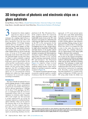
        bond pads and an optimization of the   free-form coupling scheme shown in    solder and an epoxy underfill as bonding
        reflow profile is performed to achieve   Figure 1a  requires  ≤14µm  vertical   materials. This technique is widely used
        defect-free, and high-wetting solder   distance,  whereas  the  inverse  taper   in electronic packaging industries as this
        bumps. For the inverse taper coupling   coupling method requires ≤3µm vertical   method provides both strong mechanical
        approach, the PIC is bonded to glass   distance to facilitate evanescent coupling   and electrical connections to a package
        using an ultraviolet (UV)-curable optical   as shown in Figure 1b.    [7,8]. Recently, a group demonstrated
        epoxy (n=1.5). The measured vertical   The tapered waveguide approach using   flip-chip attachment of a vertical cavity
        distance falls within the 2.8µm required   evanescent coupling requires a smaller   surface emitting laser (VCSEL) onto a Si
        Z-tolerance for evanescent coupling   Z-tolerance than the free-form coupler   PIC using solder bonds [9]. Solder was
        according to simulation.

        Introduction
          The move towards all optical I/Os on a
        switch package presents a viable solution
        for enabling low energy consumption
        (<2pJ/bit per transmitter (Tx)/receiver
        (Rx)) in devices operating at >100Gbps
        [1]. In these Tx/Rx packages, the PICs
        are co-packaged with the electronic
        integrated circuits (EICs) on a single
        interposer to minimize radio frequency
        (RF) track length [2]. This presents
        a unique opportunity for using the
        interposer material as a unified electrical-
        optical interface. Glass can be used for
        this purpose due to its low dielectric
        constant, low-loss tangent and low-
        loss optical wave guiding properties
        [3]. New optical coupling strategies   Figure 1: Packaging of PIC and EIC on a glass substrate: a) using solder bump flip-chip attachment between
        such as free-form couplers and inverse   the PIC and glass substrate to enable optical coupling by 3D printed coupler, and b) by epoxy bonding PIC and
        tapers are promising interfaces for this   glass substrate to enable evanescent coupling between PIC and glass waveguides.

        14
        14   Chip Scale Review   March  •  April  •  2024   [ChipScaleReview.com]

