Page 24 - Chip Scale Review_March-April_2024-digital
P. 24
consumption by 50%, and computing
                                                                              power by more than 30 times. For
                                                                              these reasons, CPO technology should
                                                                              be implemented once the switch data
                                                                              rate exceeds 51.2Tbps. Furthermore,
                                                                              these findings have resulted in silicon
                                                                              p ho t o n ic s  u s i n g  C P O  a s s e m bl y
                                                                              technology becoming an imperative in
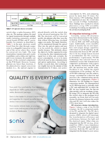
        Table 1: CPO application structure comparison.                        the advanced packaging field.

        switch chip, a radio-frequency (RF)   placed directly with the switch chip
        chip, etc. The package reduces the need   using advanced packaging like FO-  OE integration technology in CPO
        for signal transmission through multiple   EB, the electrons will be converted   Currently, various OE structures
        media (including connectors, printed   quickly into photons after they leave the   have been demonstrated in the market,
        circuit boards [PCBs], and IC carrier   chip without following long, circulated   including wire bonding, f lip chip,
        boards). For example, as described in   copper wire paths. The signal, therefore,   to fan-out RDL and 3DIC packaging
        Table 1, in the past, electrons would   will be transmitted through the optical   types. Additionally, every assembly
        travel from the chip through copper   fiber into the optical engine and pass   house or foundry has its own know-
        wires to a pluggable transceiver at the   it to the switch die, which is a much   how and unique design capability
        end of the server where they would   smaller distance. This definitely allows   with respect to an OE platform. As the
        be  converted  into  light.  The  long   the chip to be further upgraded in terms   interconnection between PIC and EIC
        intermediate transmission path results   of reducing the data transmission path,   dies is the key design feature needed
        in problems such as delay and high loss,   signal loss or delay and, certainly, the   to  accommodate  the  OE  electrical
        and it even increases the assembly cost   power consumption, so as to be more   performance requirement, FO-EB
        because of the scattered components   effectively used in data communications   technology was selected based on
        on the PCB board. However, because   and optical applications. According to   simulation results that demonstrated
        photons are faster than electrons, if   further research data, this technology   competitive performance with respect
        the photoelectric signal conversion   can roughly increase the amount of data   to the distance between the PIC and
        module (i.e., the optical engine) is   transmission by 8 times, save power   EIC, the insertion loss, and RC delay.
                                                                              Needless  to say, within  the signal
                                                                              transmission in the package, the use
                                                                              of FO-EB technology can also achieve
                                                                              energy consumption reduction and
                                                                              increases the communication speeds
                                                                              between these components. Figure 2
                                                                              illustrates the OE buildup in a signal
                                                                              conversion module. We demonstrated
                                                                              an FO-EB being used to vertically stack
                                                                              a PIC and embedded EIC in which the
                                                                              PIC die was bonded onto the fan-out
                                                                              chip module with an overhang design.
                                                                              By using CPO to integrate the OE with
                                                                              the switch chip in the package-level
                                                                              assembly, we know that will not only
                                                                              shorten the distance between the switch
                                                                              chip and OE, but it will also reduce the
                                                                              CPO’s form factor.
                                                                                OE structure design introduction.
                                                                              Figure 3 shows a map of the FO-EB
                                                                              structure: the OE is comprised mainly
                                                                              of the PIC and the EIC. The PIC die is
                                                                              designed to integrate the digital signal
                                                                              process (DSP), which will dominate
                                                                              the transformation efficiency and
                                                                              performance between the light and
                                                                              the electrical signal. Other chips are
                                                                              integrated into the EIC die (e.g., driver
                                                                              amplifier (DRV), trans-impedance
                                                                              amplifier (TIA) and signal modulator
                                                                              function). Both the PIC and EIC are
                                                                              integrated into the design to cover various


        22   Chip Scale Review   March  •  April  •  2024   [ChipScaleReview.com]
        22

