Page 26 - Chip Scale Review_March-April_2024-digital
P. 26
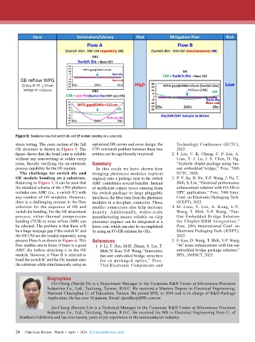
Figure 6: Simulation result of switch die and OE module bonding on a substrate.
        stress testing. The cross section of the full   optimized DB carrier and cover design, the   Technology Conference (ECTC),
        OE structure is shown in Figure 5. The   CTE mismatch problem between these two   2023.
        figure shows that the bond joint is reliable   entities can be significantly improved.   2.  J. Lin, C. K. Chung, C. F. Lin, A.
        without any non-wetting or solder creep                                   Liao, Y. J. Lu, J. S. Chen, D. Ng,
        issue, thereby verifying the on-substrate   Summary                       “Scalable chiplet package using fan-
        process capability for the OE module.  In  this  study  we  have  shown  how   out embedded bridge,” Proc. 70th
          The challenge for switch die and   bringing photonics modules (optical   ECTC, 2020.
        OE module bonding on a substrate.   engines) onto a package next to the switch   3.  P. Y. Su, D. Ho, Y-P. Wang, J. Pu, T.
        Returning to Figure 3, it can be seen that   ASIC contributes several benefits. Instead   Shih, S. Lin, “Electrical performance
        the standard scheme of the CPO platform   of inefficient copper traces running from   enhancement solution with FO-EB in
        includes one ASIC (i.e., a switch IC) with   the switch package to large pluggable   HPC application,” Proc. 24th Inter.
        any number of OE modules. However,   interfaces, the fiber runs from the photonics   Conf. on Electronic Packaging Tech.
        there is a challenging process in the flow   modules to a faceplate connector. Those   (ICEPT), 2023.
        selection for the sequence of OE and   smaller connectors also help increase   4.  M. Liao, V. Lin, A. Kang, L-Y.
        switch die bonding. For the OE attachment   density. Additionally, wafer-scale   Wang, T. Shih, Y-P. Wang, “Fan-
        process, either thermal compression   manufacturing means reliable on-chip   Out  Embedded  Bridge  Solution
        bonding (TCB) or mass reflow (MR) can   photonics engines can be integrated at a   for Chiplet/HBM Integration,”
        be selected. The problem is that there will   lower cost, which can also be accomplished   Proc. 24th International Conf. on
        be a huge warpage gap if the switch IC and   by using an FO-EB solution for OEs.  Electronic Packaging Tech. (ICEPT),
        the OE CM are die bonded separately using                                 2023.
        process Flow-A as shown in Figure 6. This   References                  5.  F. Kao, D. Wang, T. Shih, Y-P. Wang
        flow enables one to know if there is a good   1.  J. Li, T. Hsu, M-H. Zhuan, S. Lin, T.   “AC noise enhancement with fan-out
        ASIC die before attaching it to the OE   Shih, N. Kao, Y-P. Wang, “Innovative   embedded bridge package solution,”
        module. However, if Flow B is selected to   fan-out embedded bridge structure   SPIL, IMPACT, 2023.
        bond the switch IC and the OE module onto   for co-packaged optics,” Proc.
        the substrate while simultaneously using an   73rd Electronic Components and


                       Biographies
                         Chi-Ching (David) Ho is a Department Manager in the Corporate R&D Center at Siliconware Precision
                       Industries Co., Ltd., Taichung, Taiwan, R.O.C. He received a Masters Degree in Electrical Engineering,
                       National Chuanghua U. of Education, Taiwan. He joined SPIL in 2010 and is in charge of R&D Package
                       Application. He has over 20 patents. Email: davidho@SPIL.com.tw

                         Jui-Cheng (Steven) Lin is a Technical Manager in the Corporate R&D Center at Siliconware Precision
                       Industries Co., Ltd., Taichung, Taiwan, R.O.C. He received his MS in Electrical Engineering from U. of
          Southern California and has over twenty years of job experience in the semiconductor industry.


        24   Chip Scale Review   March  •  April  •  2024   [ChipScaleReview.com]
        24

