Page 49 - Chip Scale Review_January-February_2024-digital
P. 49
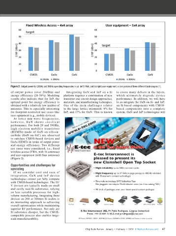
Figure 2: Output power for 28GHz and 39GHz operating frequencies in: a)  (left) FWA, and b) (right) user equipment: a comparison of three different technologies [1].
        of output power (over 20dBm) and     Integrating GaN and InP on a Si   to create many defects in the layers,
        energy efficiency (20-30%). Modeling   platform requires a combination of new   which ultimately degrade device
        results also indicate that for InP, the   transistor and circuit design approaches,   performance. In addition, we will have
        optimal point for energy efficiency is   materials, and manufacturing techniques.   to co-integrate the GaN-on-Si- and InP-
        obtained with a relatively low number of   One of the main challenges relates   on-Si-based components with CMOS-
        antennas. This is especially interesting   to the large lattice mismatch: 8% for   based  components  into  a  complete
        for footprint-restricted use cases like   InP, and 17% for GaN. This is known   system. GaN and InP technologies will
        user equipment (e.g., mobile devices).
          At  lower  mm-wave  frequencies,
        howe ve r,  G a N sh ow s e xc e l l e n t
        performance. For both 28 and 39GHz,
        high-electron mobility transistors
        (HEMTs) made of GaN-on-silicon-
        carbide (GaN-on-SiC) are observed
        to outclass CMOS-based devices and
        GaAs HEMTs in terms of output power
        and energy efficiency. Two different
        use cases were considered, i.e., fixed
        wireless access (FWA, with 16 antennas)
        and user equipment (with four antennas)
        (Figure 2).

        Opportunities and challenges for
        upscaling
          If we consider cost and ease of
        integration, GaN and In P device
        technologies cannot yet fully compete
        with CMOS-based technologies. The III/
        V devices are typically made on small
        and costly non-Si substrates, relying
        on less suitable processes for high-
        volume manufacturing. Integrating these
        devices on 200 or 300mm Si wafers is
        an interesting approach to achieving
        overall optimization while maintaining
        superior RF performance. Not only are
        Si substrates cheaper, but the CMOS-           E-Tec Interconnect  AG, Mr. Pablo Rodriguez,  Lengnau Switzerland
        compatible process also enables large-             Phone : +41 32 654 15 50, E-mail: p.rodriguez@e-tec.com
        scale manufacturability.


                                                                                                             47
                                                          Chip Scale Review   January  •  February  •  2024   [ChipScaleReview.com]  47

