Page 51 - Chip Scale Review_January-February_2024-digital
P. 51
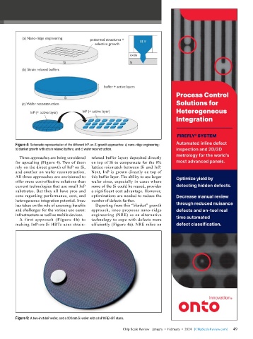
Figure 4: Schematic representation of the different InP-on-Si growth approaches: a) nano-ridge engineering;
        b) blanket growth with strain relaxed buffers, and c) wafer reconstruction.

          Three approaches are being considered   relaxed buffer layers deposited directly
        for upscaling (Figure 4). Two of them   on top of Si to compensate for the 8%
        rely on the direct growth of InP on Si,   lattice mismatch between Si and InP.
        and another on wafer reconstruction.   Next, InP is grown directly on top of
        All three approaches are envisioned to   this buffer layer. The ability to use larger
        offer more cost-effective solutions than   wafer sizes, especially in cases where
        current technologies that use small InP   some of the Si could be reused, provides
        substrates. But they all have pros and   a significant cost advantage. However,
        cons regarding performance, cost, and   optimizations are needed to reduce the
        heterogeneous integration potential. Imec   number of defects further.
        has taken on the role of assessing benefits   Departing from this “blanket” growth
        and challenges for the various use cases:   approach, imec proposes nano-ridge
        infrastructure as well as mobile devices.  engineering (NRE) as an alternative
          A first approach (Figure 4b) to   technology to cope with defects more
        making InP-on-Si HBTs uses strain-  efficiently (Figure 4a). NRE relies on


        Figure 5: A two-inch InP wafer, and a 300mm Si wafer with a InP NRE HBT stack.

                                                                                                             49
                                                          Chip Scale Review   January  •  February  •  2024   [ChipScaleReview.com]  49

