Page 50 - Chip Scale Review_January-February_2024-digital
P. 50
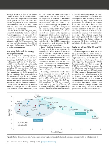
initially be used to realize the power   of innovation for power electronics   on its overall efficiency (Figure 3) [2-9].
        amplifiers within the front-end modules.   applications, the integration of GaN   Complementing  the  technology
        Also, low-noise amplifiers and switches   on large-size Si substrates has made   development with modeling activities
        could potentially benefit from the   tremendous progress. But further   will ultimately help achieve even better
        unique properties of these compound   improvements are  needed  to  ready   performance and reliability. For example,
        semiconductors. But in the end, CMOS   GaN-on-Si technology for optimal RF   at IEDM 2022, imec introduced a
        will  still be needed for calibration,   performance. The main challenges lie   simulation framework to better predict
        control, and beamforming.          in achieving comparable large signal   thermal transport in RF devices. In a
          Within its Advanced RF Program, imec,   and reliability performance to GaN-  case study with GaN-on-Si HEMTs, the
        along with its industry partners, explores   on-SiC and raising the operating   simulations revealed peak temperature
        various approaches to integrate GaN   frequency. This requires continued   rises  up  to  three  times  larger  than
        and InP devices on large-size Si wafers,   innovations in the material stack design   previously predicted. Modeling work
        and how to enable their heterogeneous   and choice of materials, reduction of the   such as this provides further guidance in
        integration with CMOS components. Pros   gate length of the HEMTs, suppression   optimizing RF devices and their layouts
        and cons are being assessed for different   of parasitics, and keeping the RF   early in the development phase [10].
        use cases—infrastructure (such as FWA)   dispersion as low as possible.
        as well as user equipment.           Imec’s GaN-on-Si process flow for   Exploring InP-on-Si for 6G sub-THz
                                           RF starts with the growth (by metal-  frequencies
        Improving GaN-on-Si technology     organic chemical vapor deposition    For the longer term, InP HBTs are
        for RF performance                 (MOCVD)) of an epitaxial structure   being explored for 6G applications. As
          Depending on the starting substrate,   on 200mm Si wafers. This structure is   previously demonstrated, of all technology
        there are several f lavors of GaN   comprised of a proprietary GaN/AlGaN   implementations, InP HBTs offer the
        technology: GaN bulk substrates, GaN-  buffer structure, a GaN channel, an   best output power/efficiency trade-off
        on-SiC, and GaN-on-Si. Today, GaN-  AlN spacer, and an AlGaN barrier. GaN   at the operating frequency of 140GHz.
        on-SiC is widely explored and already   HEMT devices with TiN Schottky metal   Researchers also know how to design InP
        used for infrastructure applications,   gates are subsequently integrated with a   HBTs for optimal RF performance. But
        including 5G base stations. GaN-on-  (low-temperature) 3-level Cu back-end-  the fabrication usually starts from small
        SiC is more cost-efficient than bulk   of-line process.               (InP) substrate wafers (<150mm), using
        GaN technology, and SiC is an excellent   Recently, competitive results have   lab-like processes that are not CMOS-
        thermal conductor that helps to dissipate   been obtained on imec’s GaN-on-Si   compatible. But what happens to the
        the generated heat in high-power   platform, bringing the output power and   performance when we integrate InP on
        infrastructure applications. However,   power added efficiency (PAE) for the   Si? Depositing InP on Si is known to
        the cost and limited size of the substrate   first time closer to those of the GaN-on-  introduce many defects, mainly threading
        make it less suitable for mass production.  SiC technology. The PAE is a commonly   dislocations and planar defects. These
          GaN-on-Si, on the contrary, has the   used metric to rate the efficiency of   defects induce leakage currents that
        potential to be upscaled to 200mm and   a power amplifier, which takes into   can dramatically deteriorate device
        even 300mm wafers. Thanks to years   account the effect of the amplifier’s gain   performance or cause reliability issues.


        Figure 3: GaN-on-Si benchmarking data. The imec data in red is among the best reported for GaN-on-Si devices and comparable to GaN-on-SiC substrates [1-9].

        48   Chip Scale Review   January  •  February  •  2024   [ChipScaleReview.com]
        48

