Page 45 - Chip Scale Review_January-February_2024-digital
P. 45
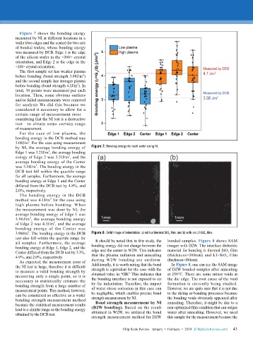
Figure 7 shows the bonding energy
        measured by NI at different locations in a
        wafer (two edges and the center) for two sets
        of bonded wafers, whose bonding energy
        was measured by DCB. Edge 1 is the edge
        of the silicon wafer in the <100> crystal
        orientation, and Edge 2 is the edge in the
        <110> crystal orientation.
          The first sample set has weaker plasma
                                       2
        before bonding (bond strength 3.08J/m )
        and the second sample has stronger plasma
                                     2
        before bonding (bond strength 4.1J/m ). In
        total, 30 points were measured per each
        location. Then, some obvious outliers
        and/or failed measurements were removed
        for analysis We did this because we
        considered it necessary to allow for a
        certain range of measurement error—
        considering that the NI test is a destructive
        test—to obtain some certain range
        of measurement.
          For the case of low plasma, the
        bonding energy in the DCB method was
              2
        3.08J/m . For the case using measurement
        by NI, the average bonding energy of   Figure 7: Bonding energy for each wafer using NI.
                       2
        Edge 1 was 3.23J/m , the average bonding
        energy of Edge 2 was 3.51J/m , and the
                                 2
        average bonding energy of the Center
                  2
        was 3.14J/m . The bonding energy in the
        DCB test fell within the quartile range
        for all samples. Furthermore, the average
        bonding energy at Edge 1 and the Center
        differed from the DCB test by 4.8%, and
        2.0%, respectively.
          The bonding energy in the DCB
        method was 4.1J/m  for the case using
                        2
        high plasma before bonding. When
        the measurement was done by NI, the
        average bonding energy of Edge 1 was
               2
        3.96J/m , the average bonding energy
                          2
        of Edge 2 was 4.3J/m , and the average
        bonding energy of the Center was
              2
        3.98J/m . The bonding energy in the DCB   Figure 8: SAM image of indentation: a) with a thermal SiO 2  film; and b) with an LT-SiO 2  film.
        test also fell within the quartile range for
        all samples. Furthermore, the average   It should be noted that in this study, the   bonded samples. Figure 8 shows SAM
        bonding energy at Edge 1, Edge 2, and the   bonding energy did not change between the   images with D2W. The interface dielectric
        Center differed from the DCB test by 3.3%,   edge and the center in W2W. This indicates   material for bonding is thermal SiO 2  film
        4.9%, and 2.0%, respectively.      that the plasma radiation and annealing   (thickness=100nm) and LT-SiO 2  film
          As expected, the measurement error of   during W2W bonding are uniform.   (thickness=100nm).
        the NI test is large, therefore it is difficult   Additionally, it is worth noting that the bond   In Figure 8, one can see the SAM image
        to measure a valid bonding strength by   strength is equivalent for the case with the   of D2W bonded samples after annealing
        measuring only a single point, so it is   obtained value in “GB.” This indicates that   at 250°C. There are some minor voids at
        necessary to statistically estimate the   the bonding interface is not exposed to air   the die edge. The root cause of the void
        bonding strength from a large number of   by the indentation. Therefore, the impact   formation is currently being studied.
        measurement points. This method, however,   of water stress corrosion in this case can   However, we are quite sure that it is not due
        can be considered as effective as a wafer   be negligible, which enables precise bond   to the dicing or bonding processes because
        bonding strength measurement method   strength measurement by NI.     the bonding voids obviously appeared after
        because the statistical measurement results   Bond strength measurement by NI   annealing. Therefore, it might be due to a
        lead to a similar range as the bonding energy   (D2W bonding). Based on the result   non-optimized film condition that can outgas
        obtained by the DCB test.          obtained in W2W, we utilized the bond   water after annealing. However, we used
                                           strength measurement method for D2W   this sample for the measurement because the

                                                                                                             43
                                                          Chip Scale Review   January  •  February  •  2024   [ChipScaleReview.com]  43

