Page 43 - Chip Scale Review_January-February_2024-digital
P. 43
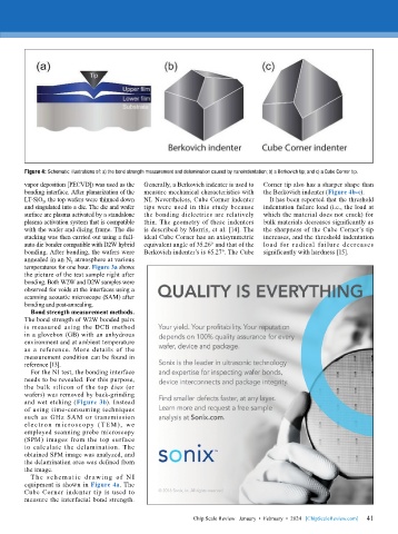
Figure 4: Schematic illustrations of: a) the bond strength measurement and delamination caused by nanoindentation; b) a Berkovich tip; and c) a Cube Corner tip.
        vapor deposition [PECVD]) was used as the   Generally, a Berkovich indenter is used to   Corner tip also has a sharper shape than
        bonding interface. After planarization of the   measure mechanical characteristics with   the Berkovich indenter (Figure 4b-c).
        LT-SiO 2 , the top wafers were thinned down   NI. Nevertheless, Cube Corner indenter   It has been reported that the threshold
        and singulated into a die. The die and wafer   tips were used in this study because   indentation failure load (i.e., the load at
        surface are plasma activated by a standalone   the bonding dielectrics are relatively   which the material does not crack) for
        plasma activation system that is compatible   thin. The geometry of these indenters   bulk materials decreases significantly as
        with the wafer and dicing frame. The die   is described by Morris, et al. [14]. The   the sharpness of the Cube Corner’s tip
        stacking was then carried out using a full-  ideal Cube Corner has an axisymmetric   increases, and the threshold indentation
        auto die bonder compatible with D2W hybrid   equivalent angle of 35.26° and that of the   load for radical failure decreases
        bonding. After bonding, the wafers were   Berkovich indenter’s is 65.27°. The Cube   significantly with hardness [15].
        annealed in an N 2  atmosphere at various
        temperatures for one hour. Figure 3a shows
        the picture of the test sample right after
        bonding. Both W2W and D2W samples were
        observed for voids at the interfaces using a
        scanning acoustic microscope (SAM) after
        bonding and post-annealing.
          Bond strength measurement methods.
        The bond strength of W2W bonded pairs
        is  measured  using  the  DCB  method
        in a glovebox (GB) with an anhydrous
        environment and at ambient temperature
        as a reference.  More details of the
        measurement condition can be found in
        reference [13].
          For the NI test, the bonding interface
        needs to be revealed. For this purpose,
        the bulk silicon of the top dies (or
        wafers) was removed by back-grinding
        and wet etching (Figure 3b). Instead
        of using time-consuming techniques
        such as GHz SAM or transmission
        elect ron m icroscopy (T EM ), we
        employed scanning probe microscopy
        (SPM) images from the top surface
        to calculate the delamination. The
        obtained SPM image was analyzed, and
        the delamination area was defined from
        the image.
          T he s che m at ic d r aw i ng of N I
        equipment is shown in Figure 4a. The
        Cube Corner indenter tip is used to
        measure the interfacial bond strength.

                                                                                                             41
                                                          Chip Scale Review   January  •  February  •  2024   [ChipScaleReview.com]  41

