Page 41 - Chip Scale Review_January-February_2024-digital
P. 41
Exploring bond strength for an advanced chiplet with


        hybrid bonding


        By Junya Fuse, Tomoya Iwata, Yuki Yoshihara, Marie Sano, Fumihiro Inoue  [YOKOHAMA National University]
        B         ecause of the high demand


                  for high-density vertical
                  intercon nections using
        advanced chiplet technology, hybrid
        bonding is now being comprehensively
        investigated as an alternative to micro-
        bumps. However, there are many
        obstacles and challenges in the R&D
        phase that remain to be overcome with
        respect to die-level hybrid bonding.
        For example, a bonding st rength
        measurement method for die-level
        hybrid bonding has not yet been well
        established. Therefore, the bonding
        strength measurement method at the die
        level was studied using the Cube Corner
        indentation method. The validity of the
        nanoindentation test was demonstrated
        by comparing the bonding strength
        calculated by using double-cantilever-
        beam and nanoindentation tests. Then,
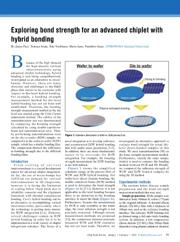
        by performing nanoindentation tests   Figure 1: Schematic illustrations of W2W vs. D2W process flow.
        on the die-to-wafer (D2W) sample, we
        compared it to the wafer-to-wafer (W2W)   novel integration is to develop collective   investigated an alternative approach to
        sample, which has a similar bonding film.   and reconstructed D2W hybrid bonding   evaluate bond strength for actual die-
        The comparison showed the difference   that will enable mass production [3-5].   level direct-bonded samples in this
        in bonding strength due to the different   In addition, there are many fundamental   study. We used nanoindentation (NI) as
        bonding films.                     issue s t o b e ove rcome for D2W   the bond strength measurement method.
                                           integration. For example, the bonding   Furthermore, exactly the same sample
        Introduction                       strength measurement for D2W bonding   (wafer) is used to compare the bonding
          P i t c h s c a l i n g o f v e r t i c a l   is not well defined.  method between DCB and NI. Finally,
        interconnections is a crucial development   Figure 1 shows the simplif ied   we compared the adhesion strength of
        aspect for advanced chiplet integration.   schematic image of the process flow of   W2W and D2W bonded samples by
        So far, the use of micro-bumps has   W2W and D2W hybrid bonding. For   using the NI method.
        f ulf illed the demand for ver tical   wafer-level direct (fusion) bonding, the
        interconnections in 3D integration,   double-cantilever-beam (DCB) method   Experimental methods
        however, it is facing the limitation   is used to determine the bond strength   The sections below discuss sample
        of  scaling  below  10μm  pitch  due  to   (Figure 2a-b) [7-11]. However, it is not   preparation and the bond strength
        reliability concerns and the alignment   applicable to die-level bonding because   measurement methods that were used.
        limitation with thermal compression   there is no initiation at the bonding   Sample preparation. All the samples were
        bonding. Cu-Cu hybrid bonding can be   interface to insert the blade (Figure 2c).   fabricated from 300mm Si wafers (775μm)
        an alternative to accomplishing vertical   Furthermore, because the measurement   as the original substrate. A thermal silicon
        interconnections, particularly where   by DCB is only available at the wafer   dioxide (Th-SiO 2 ) film with a thickness of
        the technology is getting more mature   edge, the inner adhesion strength is not   100nm was used as the reference bonding
        for W2W integration [1-2]. However,   precisely measured. Although several   interface. The reference W2W bonding was
        several challenges remain in D2W   measurement  methods  are  proposed   performed using a full-auto wafer bonding
        hybrid bonding in order for it to be   [12], the comparison between precisely   system. In addition, a low-temperature
        implemented in a wide variety of chiplet   measured W2W and D2W examples   silicon dioxide (LT-SiO 2 ) film 100nm thick
        integration schemes. The focus of a   has not yet been made. Therefore, we   (deposited using plasma-enhanced chemical

                                                                                                             39
                                                          Chip Scale Review   January  •  February  •  2024   [ChipScaleReview.com]  39

