Page 44 - Chip Scale Review_January-February_2024-digital
P. 44
Results and discussion
                                                                                The sections below discuss the precise
                                                                              bond energy measurement done by DCB
                                                                              and by NI.
                                                                                Precise bond energy measurement by
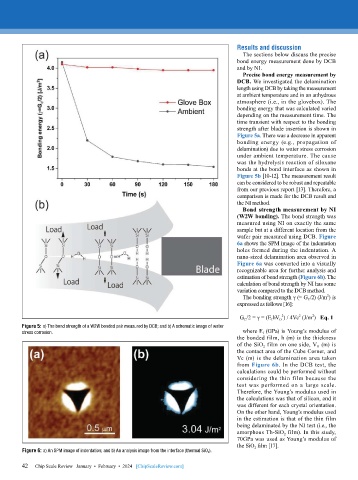
                                                                              DCB. We investigated the delamination
                                                                              length using DCB by taking the measurement
                                                                              at ambient temperature and in an anhydrous
                                                                              atmosphere (i.e., in the glovebox). The
                                                                              bonding energy that was calculated varied
                                                                              depending on the measurement time. The
                                                                              time transient with respect to the bonding
                                                                              strength after blade insertion is shown in
                                                                              Figure 5a. There was a decrease in apparent
                                                                              bonding energy (e.g., propagation of
                                                                              delamination) due to water stress corrosion
                                                                              under ambient temperature. The cause
                                                                              was the hydrolysis reaction of siloxane
                                                                              bonds at the bond interface as shown in
                                                                              Figure 5b [10-12]. The measurement result
                                                                              can be considered to be robust and repeatable
                                                                              from our previous report [13]. Therefore, a
                                                                              comparison is made for the DCB result and
                                                                              the NI method.
                                                                                Bond strength measurement by NI
                                                                              (W2W bonding). The bond strength was
                                                                              measured using NI on exactly the same
                                                                              sample but at a different location from the
                                                                              wafer pair measured using DCB. Figure
                                                                              6a shows the SPM image of the indentation
                                                                              holes formed during the indentation. A
                                                                              nano-sized delamination area observed in
                                                                              Figure 6a was converted into a visually
                                                                              recognizable area for further analysis and
                                                                              estimation of bond strength (Figure 6b). The
                                                                              calculation of bond strength by NI has some
                                                                              variation compared to the DCB method.
                                                                                The bonding strength γ (= G C /2) (J/m ) is
                                                                                                            2
                                                                              expressed as follows [16]:
                                                                               G C /2 = γ = (E f hV O ) / 4Vc  (J/m )   Eq. 1
                                                                                                       2
                                                                                                   2
                                                                                             2
        Figure 5: a) The bond strength of a W2W bonded pair measured by DCB; and b) A schematic image of water
        stress corrosion.                                                       where E f  (GPa) is Young’s modulus of
                                                                              the bonded film, h (m) is the thickness
                                                                              of the SiO 2  film on one side, V O  (m) is
                                                                              the contact area of the Cube Corner, and
                                                                              Vc (m) is the delamination area taken
                                                                              from Figure 6b. In the DCB test, the
                                                                              calculations could be performed without
                                                                              considering the thin film because the
                                                                              test was performed on a large scale.
                                                                              Therefore, the Young’s modulus used in
                                                                              the calculations was that of silicon, and it
                                                                              was different for each crystal orientation.
                                                                              On the other hand, Young’s modulus used
                                                                              in the estimation is that of the thin film
                                                                              being delaminated by the NI test (i.e., the
                                                                              amorphous Th-SiO 2  film). In this study,
                                                                              70GPa was used as Young’s modulus of
                                                                              the SiO 2  film [17].
        Figure 6: a) An SPM image of indentation; and b) An analysis image from the interface (thermal SiO 2 ).

        42
        42   Chip Scale Review   January  •  February  •  2024   [ChipScaleReview.com]

