Page 40 - Chip Scale Review_January-February_2024-digital
P. 40
To resolve the above challenge, the
                                                                              xSI and Calibre 3DSTACK currently
                                                                              include a plug-in that allows the
                                                                              system-level desig ner to ut ili ze
                                                                              the information stored in the xSI
                                                                              database to automatically generate a
                                                                              complete Calibre 3DSTACK runset
                                                                              (f u l l  a s s e m bl y d e s c r i p t io n a n d
                                                                              comprehensive assembly  checks)
                                                                              along with a system source netlist.
                                                                              T h i s de sig ne r- c e nt r ic ap p ro a ch
                                                                              i s a g no st ic t o t he d i f fe r e nt d ie
                                                                              t e ch nolog y node s, t he d if fe re nt
                                                                              substrates involved in the assembly,
                                                                              and the different manufact u r ing
                                                                              ve ndor s (for ex a mple, a si l ic on
                                                                              interposer from foundry X and an
                                                                              organic substrate from OSAT Y).

                                                                              Summary
                                                                                For 3D-IC assemblies, the designer
                                                                              must ensure that the system-level netlist
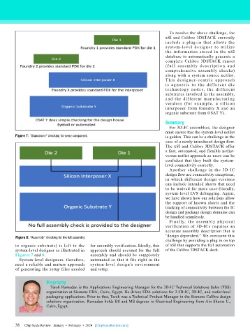
        Figure 7: “Standalone” checking for every component.                  is golden. This can be a challenge in the
                                                                              case of a newly-introduced design flow.
                                                                              The xSI and Calibre 3DSTACK offer
                                                                              a fast, automated, and flexible netlist-
                                                                              versus-netlist approach so users can be
                                                                              confident that they built the system-
                                                                              level connectivity correctly.
                                                                                Another challenge in the 3D-IC
                                                                              design flow are connectivity exceptions,
                                                                              in which different design versions
                                                                              can include intended shorts that need
                                                                              to be waived for more user-friendly,
                                                                              system-level LVS debugging. Again,
                                                                              we have shown how our solutions allow
                                                                              the support of known shorts and the
                                                                              tracking of connectivity between the IC
                                                                              design and package design domains can
                                                                              be handled seamlessly.
                                                                                Finally, the assembly physical
                                                                              verification of 3D-ICs  requires an
                                                                              accurate assembly description that is
                                                                              “design dependent.” We overcame this
        Figure 8: “Assembly” checking for the full assembly.
                                                                              challenge by providing a plug in on top
        to organic substrate) is left to the   for assembly verification. Ideally, this   of xSI that supports the full automation
        system-level designer as illustrated in   approach should account for the full   of the Calibre 3DSTACK deck.
        Figures 7 and 8.                   assembly and should be completely
          System-level designers, therefore,   automated so that it fits right in the
        need a reliable and mature approach   system-level design’s environment
        of generating the setup files needed   and setup.


                       Biography
                         Tarek Ramadan is the Applications Engineering Manager for the 3D-IC Technical Solutions Sales (TSS)
                       organization at Siemens EDA, Cairo, Egypt. He drives EDA solutions for 2.5D-IC, 3D-IC, and wafer-level
                       packaging applications. Prior to that, Tarek was a Technical Product Manager in the Siemens Calibre design
                       solutions organization. Ramadan holds BS and MS degrees in Electrical Engineering from Ain Shams U.,
                       Cairo, Egypt.


        38   Chip Scale Review   January  •  February  •  2024   [ChipScaleReview.com]
        38

