Page 35 - Chip Scale Review_January-February_2024-digital
P. 35
Making the golden connections in 3D-IC


        system-level design


        By Tarek Ramadan  [Siemens EDA]
        3       D integration is becoming


                a valuable alternative to the
                ongoing, yet challenging,
        transistor scaling known as Moore’s
        Law. T h is is especially t r ue for
        semiconductor products that are
        becoming limited by single-die designs
        (e.g., in terms of form factor, size, and
        technology node).  Homogeneous 2.5D
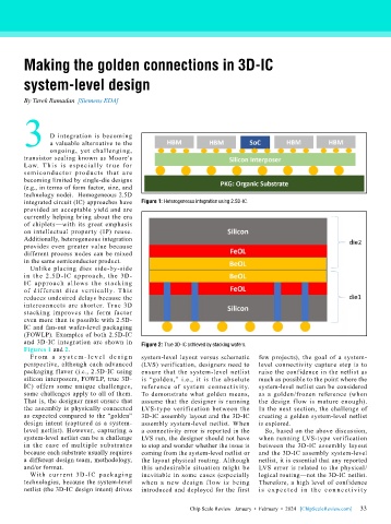
        integrated circuit (IC) approaches have   Figure 1: Heterogeneous integration using 2.5D-IC.
        provided an acceptable yield and are
        currently helping bring about the era
        of chiplets—with its great emphasis
        on intellectual property (IP) reuse.
        Additionally, heterogeneous integration
        provides even greater value because
        different process nodes can be mixed
        in the same semiconductor product.
          Unlike placing dies side-by-side
        in the 2.5D-IC approach, the 3D-
        IC approach allows the stack ing
        of different dies ver tically. This
        reduces undesired delays because the
        interconnects are shorter. True 3D
        stacking improves the form factor
        even more than is possible with 2.5D-
        IC and fan-out wafer-level packaging
        (FOWLP). Examples of both 2.5D-IC
        and 3D-IC integration are shown in   Figure 2: True 3D-IC achieved by stacking wafers.
        Figures 1 and 2.
          F r o m a s y s t e m - l e v e l d e s i g n   system-level layout versus schematic   few projects), the goal of a system-
        perspective, although each advanced   (LVS) verification, designers need to   level connectivity capture step is to
        packaging flavor (i.e., 2.5D-IC using   ensure that the system-level netlist   raise the confidence in the netlist as
        silicon interposers, FOWLP, true 3D-  is “golden,” i.e., it is the absolute   much as possible to the point where the
        IC) offers some unique challenges,   reference of system connectivity.   system-level netlist can be considered
        some challenges apply to all of them.   To demonstrate what golden means,   as a golden/frozen reference (when
        That is, the designer must ensure that   assume that the designer is running   the design f low is mature enough).
        the assembly is physically connected   LVS-type verification between the   In the next section, the challenge of
        as expected compared to the “golden”   3D-IC assembly layout and the 3D-IC   creating a golden system-level netlist
        design intent (captured as a system-  assembly system-level netlist. When   is explored.
        level netlist). However, capturing a   a connectivity error is reported in the   So, based on the above discussion,
        system-level netlist can be a challenge   LVS run, the designer should not have   when running LVS-type verification
        in the case of multiple substrates   to stop and wonder whether the issue is   between  the 3D-IC  assembly  layout
        because each substrate usually requires   coming from the system-level netlist or   and the 3D-IC assembly system-level
        a different design team, methodology,   the layout physical routing. Although   netlist, it is essential that any reported
        and/or format.                     this undesirable situation might be   LVS error is related to the physical/
          With cu r rent 3D -IC packaging   inevitable in some cases (especially   logical routing—not the 3D-IC netlist.
        technologies, because the system-level   when a new design f low is being   Therefore, a high level of confidence
        netlist (the 3D-IC design intent) drives   introduced and deployed for the first   is ex p e ct e d i n t he c on ne ct iv it y

                                                                                                             33
                                                          Chip Scale Review   January  •  February  •  2024   [ChipScaleReview.com]  33

