Page 33 - Chip Scale Review_January-February_2024-digital
P. 33
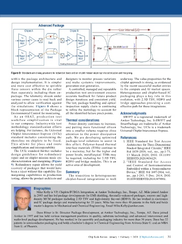
Figure 9: Standards are driving provisions for redundant lanes and on-chiplet mission mode eye characterization and margining.
        within the package architecture and   designers to monitor process variations   underway. The value proposition for the
        design implementation. It is simpler   and make systemic improvements,   chiplet approach is strong, as evidenced
        and more cost effective to sprinkle   generation over generation.     by the recent successful market entries
        these  sensors within the  die rather   A controlled, managed and repeatable   in the compute and AI market spaces.
        than separately including them on-  production test environment ensures   Heterogeneous and chiplet-based IC
        package. The telemetry stream under   accurate feedback for future product   packaging plays a key role in this
        various corner cases is read back and   design iterations and consistent yield.   evolution, with 2.5D TSV, HDFO and
        analyzed to allow verification against   The test, package handling and optical   bridge approaches providing a cost-
        the simulations.  Figure  8 shows a   inspection supply chain is continuing   effective path for these integrations.
        block representation of the Package   to refine the metrology to account for
        Environmental Control for monitoring.  all the identified failure pinch points.  Acknowledgments
          A s a n O SAT, p r o d u c t io n t e s t                             SWIFT is a registered trademark of
        work f low simplif ication is vit al   Thermal considerations         Amkor Technology, Inc. S-SWIFT and
        to our company. Industrywide test    Power density continues to increase,   SmartPackage are trademarks of Amkor
        methodology standardization efforts   and  putting  more  functional  silicon   Technology, Inc. UCIe is a trademark
        are helping. For instance, the Universal   into a smaller volume requires close   Universal Chiplet Interconnect Express.
        Chiplet Interconnect Express (UCIe)   attention to the power dissipation
        standard includes constraining the   path. We are developing optimized   References
        shoreline on chiplets to be fixed.   package-level solutions to assist in   1.  IEEE  Standard  for  Test  Access
        T h is al lows for pla ce a nd rout e   this  effort.  Polymer-based  thermal   Architecture for Three-Dimensional
        simplification and interoperability.  interface materials (TIMs) continue to   Stacked Integrated Circuits,” IEEE
          The UCIe standard further includes   be a mainstay, but for the higher end   Std 1838-2019, vol., no., pp.1-73,
        design guidelines for redundancy   power levels, metallurgical TIMs may   13 March 2020, DOI: 10.1109/
        repair and on-chiplet mission mode eye   be required, including for 2.5D TSV,   IEEESTD.2020.9036129.
        characterization and margining (Figure   HDFO and bridge modules. This is an   2.  ” I E E E St a n d a r d fo r Ac c e s s
        9). Redundancy repair allows for yield   active area of development.      and Control  of Instrumentation
        recovery of packages that would have                                      Embedded within a Semiconductor
        been a reject without this capability. Eye   Summary                      Device,” IEEE Std 1687-2014, vol.,
        margining capabilities in production   The  transition  to  heterogeneous   no., pp.1-283, 5 Dec. 2014, DOI:
        testing, allows the product architects and   chiplet-based integrations is well   10.1109/IEEESTD.2014.6974961.


                       Biographies
                         Mike Kelly is VP, Chiplets/FCBGA Integration, at Amkor Technology, Inc., Tempe, AZ. Mike joined Amkor
                       in 2005 and has led package developments for EMI shielding, thermally-enhanced packages, sensors and high-
                       density MCM packages including 2.5D TSV and high-density fan-out (HDFO). He has worked in electronics
                       and IC package design and manufacturing for 25 years. Mike has more than 40 patents in the field and holds
                       master’s degrees in Mechanical and Chemical Engineering. Email Mike.Kelly@amkor.com.
                         Dave Hiner is Sr. Director Package Development, at Amkor Technology, Inc., Tempe, AZ. Dave joined
          Amkor in 1997 and has held various management positions in quality, substrate technology and advanced interconnect and
          wafer-level package development. He has worked in the assembly and packaging industry for more than 30 years. Dave has 22
          patents in semiconductor packaging and holds a bachelor’s degree in Chemical Engineering from Arizona State U. and an MBA
          from U. of Phoenix.


                                                                                                             31
                                                          Chip Scale Review   January  •  February  •  2024   [ChipScaleReview.com]  31

