Page 28 - Chip Scale Review_January-February_2024-digital
P. 28
HDFO
          Modules based on HDFO interposers
        have been internally qualified and
        several  of  our  customers’  products
        are in qualification. Our internal
        terminology for HDFO is S-SWIFT
        (Substrate  Silicon  Wafer Integrated
        F a n - o u t  Te c h n o log y ) .  H D F O
        technology is being applied to many
        markets and use applications, ranging
        f rom high-per for mance compute
        and AI, to automotive applications
        and beyond. Chiplet architectures
        are leading to a push for advanced
        pack ag i ng desig n  r u les  t hat  a re
        enabled by HDFO and other module-
        based solutions. Our fabrication of
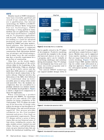
        this HDFO interposer is supported   Figure 2: General chip-first vs. chip-last flow.
        in both a chip-first and a chip-last   that is equally critical to the TV phase   1.5-micron line and 1.5-micron space
        construction. Each fabrication method   of development. Predictive modeling   and with layer counts between 2 and 6
        has advantages and disadvantages,   can provide key insights to the design   layers. Module sizes can be supported
        and in many cases the end customer   and material choices at the start of   from smaller modules, to modules
        may have a specific requirement for a   a program, and it can be valuable at   that are larger than reticle size using
        given flow or construction.        identifying challenges and solutions   reticle stitching.  Figure 3 shows a
          Chip f irst, as the words imply,   during development. This TV strategy   typical 6-layer RDL module with the
        involves the placement of the active   for development has been used over   top die solder joint fabricated in a
        silicon chips at the beginning of the   many successful programs and is   chip-last approach.  Figure 4 shows
        module fabrication. Chips are attached   highly recommended.          the subsequent module to substrate
        face up on a wafer carrier and the   Our cur rent SWIFT technology    solder joint.
        multi-layer RDL process is completed   can support module designs down to
        with direct metal connections to the
        active silicon. Chip last involves the
        fabrication of the RDL first followed
        b y a t r a d i t i o n a l c h i p - o n -wa fe r
        assembly process using solder joints
        and underfill. Once the modules are
        completed, they are assembled to a
        package substrate in a manner similar
        to non-module-based products. Figure
        2 shows a high-level comparison of
        these two approaches.
          W h e n c o n s i d e r i n g a p r o d u c t
        intercept into HDFO, we encourage
        the use of a test vehicle (TV) that
        matches the design complexity of the
        final product. This TV phase can make
        use of the hierarchy of design rules
        within the design to test boundaries of   Figure 3: Test vehicle die connected to HDFO.
        HVM design rules and overall process
        capability.  This  process  provides
        va l id at ion for t he f i r st pro d uc t
        intercept and gives a first check on
        next-generation requirements. These
        TV designs utilize a series of daisy
        chains that can test historical areas of
        high stress, including die corners, die
        gaps, module corners, stacked vias and
        others. Having a well-defined daisy
        chain can give electrical data that can
        bolster the mechanical modeling work
                                           Figure 4: Test vehicle HDFO module connected to package substrate.

        26
        26   Chip Scale Review   January  •  February  •  2024   [ChipScaleReview.com]

