Page 30 - Chip Scale Review_January-February_2024-digital
P. 30
Bridges                            maturity levels can often influence the   layout early in the design flow process
          The next iteration of HDFO enables   decision making of our customers.  can significantly facilitate a smooth
        a 3D capability using bridge silicon   Our version (S-Connect) of the   supply chain support path. Notably, this
        and other embedded components under   embedded bridge HDFO module on   solution is compatible with multiple
        the active silicon. The fundamental   substrate is shown in  Figure 5. We   electronic design automation (EDA)
        building blocks developed in HDFO   have completed internal qualification   design tools, further securing the
        interposer fabrication are extended   of a chip-last non-TSV bridge TV, and   ability to align with many independent
        w it h t he i nclu sion of embedded   we are working with several customers   design workflows.
        bridging components or other devices.   on plans  to  utilize  these  advanced   Two prevalent design workflows in
        These  embedded  components  can   capabilities.                      contemporary practices are the Full-
        have a basic ultra-high density routing                               OSAT f low and the OEM/Fabless-
        function, such as between two chiplets,   Design support              focused project-based design processes.
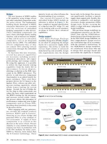
        or they can be active or non-active   O u r  Sm a r t P a c k a g e  P a c k a g e   In the Full-OSAT design workflow, we
        components, such as an integrated   Assembly Design Kits (PADK) (Figure   have comprehensive design services
        passive device (IPD). The embedded   6) are ideal for preparing the design   and verification sign-off in accordance
        sil icon  component s  may  or  may   layout for a successful supply chain   with the customer’s instructions. In
        not contain TSVs allowing vertical   experience. The ability to build the   the OEM/Fabless design workf low,
        connections through the embedded   various high-volume or advanced    we collaborate with users who opt
        components.                        manufacturing and assembly design   to design their package layout and
          To facilitate this new structure,   rule requirements into the design   necessitate the capability to finalize
        several key process capabilit ies
        are necessar y including accurate
        component placement, tall copper
        pillar  plating,  and warpage control.
        By using this approach, it is possible
        to utilize the high-density routing
        capabilit y f rom the wafer fab to
        i n ter c o n n ec t   b e t we e n   c h i ple t s ,
        allowing a reduction in the RDL layer
        count in the HDFO interposer. The
        ability to add discrete component
        functionality is an added benefit for
        many customers. There exist three
        primary drivers for S-Connect in the
        market. First, silicon can offer sub-
        micron routing capability, which
        allows denser routing for system
        design.  Second, the use of bridge die
        for the chip-to-chip connections can
        reduce the layer count requirement on
        the HDFO routing for the interposer
        and increase overall yields. Lastly,   Figure 5: Amkor’s S-Connect Technology.
        the process allows the placement of
        performance-enhancing non-bridge
        components such as silicon IPDs,
        providing closer proximity to key areas
        of the active silicon.
          When engaging with our customers,
        we consider the tradeoff analysis
        b e t we e n H DFO a nd S - C o n ne c t .
        Sourcing of the silicon bridge and
        potential IPDs is a key element of
        this assessment. A supply of these
        components is as cr it ical to t he
        decision as the active silicon. Process
        maturity is a key element because the
        industry has been in production with
        2.5D TSV modules for many years.
        HDFO is, likewise, more mature than
        the  S-Connect technology. These
                                           Figure 6: Amkor’s SmartPackage PADK fine-tuned customized design rule requirements.

        28
        28   Chip Scale Review   January  •  February  •  2024   [ChipScaleReview.com]

