Page 32 - Chip Scale Review_January-February_2024-digital
P. 32
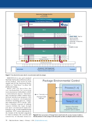
Figure 7: Production test for power, data I/O, bias and clocks in multi-die packages.
          IEEE1838 [1] is one such standard
        that helps during the architecture phase
        of the product. Test access to each
        chiplet and all the functional blocks
        within is a “must have,” to allow full
        production testing.
          I E E E -16 8 7 [ 2] d e s c r i b e s t h e
        t e s t me t ho dolog y for a c c e s si ng
        instrumentation  embedded within
        a semiconductor device. Electronic
        data automation (EDA) vendors have
        defined intellectual  property  (IP)
        blocks to monitor environmental
        attributes including process, voltage
        and temperature (PVT) on-die. They
        have a similar concept of adding
        se n sor s w it h i n t he log ic de sig n
        a nd have docu ment ed nu me rou s
        benefits to the overall manufacturing
        workflow. PVT sensor placement in
        the vicinity of the thermal congestion
        is vital to analyze the severity and   Figure 8: Block representation of Package Environmental Control with a variety of sensors that allow a
        se n sit iv it y of t he r m al de n sit ie s   telemetry stream to monitor package health during active operation, including the production test process.

        30   Chip Scale Review   January  •  February  •  2024   [ChipScaleReview.com]
        30

