Page 39 - Chip Scale Review_January-February_2024-digital
P. 39
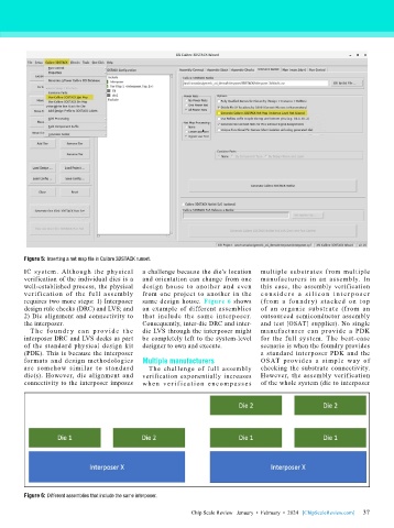
Figure 5: Inserting a net map file in Calibre 3DSTACK runset.

        IC system. Although the physical   a challenge because the die’s location   multiple substrates from multiple
        verification of the individual dies is a   and orientation can change from one   manufacturers in an assembly. In
        well-established process, the physical   design house to another and even   this  case,  the  assembly  verification
        verif ication of the f ull assembly   from  one  project  to  another  in  the   c o n s i d er s  a  s i li c o n  i n t er p o s er
        requires two more steps: 1) Interposer   same design house. Figure 6 shows   (f rom a fou nd r y) st acked on top
        design rule checks (DRC) and LVS; and   an example of different assemblies   of an organic subst rate (f rom an
        2) Die alignment and connectivity to   that include the same inter poser.   outsourced semiconductor assembly
        the interposer.                    Consequently, inter-die DRC and inter-  and test [OSAT] supplier). No single
          T h e fo u n d r y c a n p r ov i d e t h e   die LVS through the interposer might   manufacturer can provide a PDK
        interposer DRC and LVS decks as part   be completely left to the system-level   for the  full system.  The  best-case
        of the standard physical design kit   designer to own and execute.    scenario is when the foundry provides
        (PDK). This is because the interposer                                 a standard interposer PDK and the
        formats and design methodologies   Multiple manufacturers             OSAT prov ides a si mple way of
        are somehow similar to standard      The challenge of full assembly   checking the substrate connectivity.
        die(s). However, die  alignment and   verification exponentially increases   However, the assembly verification
        connectivity to the interposer imposes   whe n ve r i f ic a t io n e n c om p a s s e s   of the whole system (die to interposer


        Figure 6: Different assemblies that include the same interposer.

                                                                                                             37
                                                          Chip Scale Review   January  •  February  •  2024   [ChipScaleReview.com]  37

