Page 48 - Chip Scale Review_January-February_2024-digital
P. 48
Scaling up GaN- and InP-based technologies for 5G


        and 6G wireless communication


        By Nadine Collaert  [imec]
        Y         ear after year, more and   fraction of transmitted energy reaches   power and efficiency at high operating


                  m o r e  d a t a a r e  b e i n g
                  transmitted wirelessly by   the intended receiver.          frequencies. GaN, for example, has
                                                                              a high current density, high electron
                                             The advent of higher frequencies,
        an ever-growing group of users. To   however, comes at a price. Today,   mobility, and large breakdown voltage.
        keep up with this trend and make data   c o m p l e me n t a r y  me t a l - o x i d e -  The high power density also allows for
        transfer faster and more efficiently,   semiconductor (CMOS) is the preferred   a small form factor and, therefore, a
        the fifth generation (5G) of mobile   technology for building the critical   reduction in overall system size at the
        communication is being rolled out, and   component s of t r a n sm it te r s a nd   same performance.
        the industry is already looking at what   receivers. These  include  the  power
        lies beyond. While 5G enables peak   amplifiers within the front-end modules   GaN and InP outclass CMOS at
        data rates of 10Gbit/s, 6G is projected   that send the radio frequency signals   higher operating frequencies
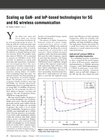
        to operate at 100Gbit/s from 2030   to and from the antennas. The higher   In a modeling exercise, researchers
        onwards. In addition to coping with   the operating frequency, the more the   at imec compared the performance
        more data and connections, researchers   CMOS-based power amplifiers struggle   of three different power amplifier
        a r e i nve s t ig a t i ng how t h e n e x t   to deliver the required output power   implementations at 140GHz operating
        generation of wireless communication   with sufficiently high efficiency. And   frequency: a full CMOS implementation,
        can support new use cases such as   that’s where technologies such as GaN   a CMOS be a m for me r w it h SiGe
        autonomous driving and holographic   and InP come into play. Because of   heterojunction bipolar t ransistor
        presence, among others. To enable   their outstanding material properties,   (HBT), and an InP HBT (Figure 1)
        these exceedingly high data rates, the   these III/V semiconductors are more   [1]. InP was the clear winner in terms
        telecom industry has been pushing up   likely to provide the required output
        the  frequencies  of  wireless  signals.
        While 5G initially uses sub-6GHz
        frequency bands, products targeting
        28/39GHz are already showcased.
        Additionally, there is a growing interest
        in using FR3 (6-20GHz) frequency
        bands for  5G networks  because  of
        their ability to balance coverage and
        capacity. For 6G, frequencies above
        100GHz are being discussed.
          Moving toward higher frequencies
        has several advantages: new frequency
        bands can be used—thereby solving the
        spectrum scarcity issue within existing
        bands. Also, the higher the operating
        frequency, the easier it is to obtain
        wider bandwidths. Frequencies above
        100GHz and bandwidths up to 30GHz
        allow telecom operators, in principle,
        to use lower-order modulation schemes
        within the wireless data links, which
        reduces power consumption. Higher
        frequencies are also associated with
        smaller wavelengths (λ). As the antenna
                           2
        array size scales with λ , antenna arrays
        can be packed more densely. This
        contributes to better beamforming, a
        technique that ensures that a larger   Figure 1: Comparing the power consumption of CMOS, SiGe, and InP devices in transmitter architectures as a
                                           function of the number of antennas [1].
        46   Chip Scale Review   January  •  February  •  2024   [ChipScaleReview.com]
        46

