Page 46 - Chip Scale Review_January-February_2024-digital
P. 46
Summary
                                                                                The investigation of an alternative
                                                                              approach to evaluate bond strength for
                                                                              actual die-level direct bonded samples was
                                                                              executed. The estimation of bond strength
                                                                              at the die level is crucial in assessing the
                                                                              reliability of advanced chiplets processed
                                                                              using D2W hybrid bonding. The use of the
                                                                              nanoindentation test made it possible to
                                                                              measure the in-plane uniformity of W2W
                                                                              bonding. Furthermore, it is now possible
                                                                              to measure the bonding strength of D2W
                                                                              samples, which could not be measured
                                                                              in the DCB test. Although the accuracy
                                                                              of the measurement is still a challenge,
                                                                              the measurement can accelerate the
                                                                              development of D2W hybrid bonding with a
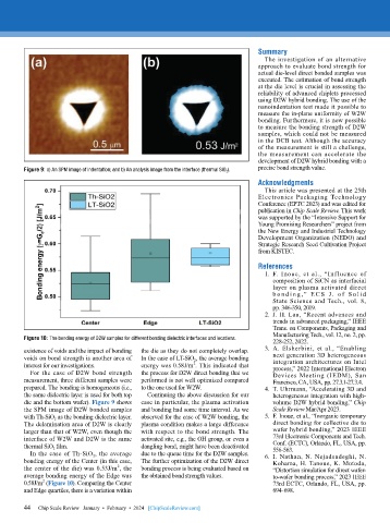
        Figure 9: a) An SPM image of indentation; and b) An analysis image from the interface (thermal SiO 2 ).  precise bond strength value.
                                                                              Acknowledgments
                                                                                This article was presented at the 25th
                                                                              Electronics Packaging Technology
                                                                              Conference (EPTC 2023) and was edited for
                                                                              publication in Chip Scale Review. This work
                                                                              was supported by the “Intensive Support for
                                                                              Young Promising Researchers” project from
                                                                              the New Energy and Industrial Technology
                                                                              Development Organization (NEDO) and
                                                                              Strategic Research Seed Cultivation Project
                                                                              from KISTEC.

                                                                              References
                                                                                1.  F. Inoue, et al., “Inf luence of
                                                                                   composition of SiCN as interfacial
                                                                                   layer on plasma activated direct
                                                                                   b o n d i ng ,” E C S J. of S o l i d
                                                                                   State Science and Tech., vol. 8,
                                                                                   pp. 346-350, 2019.
                                                                                2.  J. H. Lau, “Recent advances and
                                                                                   trends in advanced packaging,” IEEE
                                                                                   Trans. on Components, Packaging and
                                                                                   Manufacturing Tech., vol. 12, no. 2, pp.
        Figure 10: The bonding energy of D2W samples for different bonding dielectric interfaces and locations.
                                                                                   228-252, 2022.
        existence of voids and the impact of bonding   the die as they do not completely overlap.   3.  A. Elsherbini, et al., “Enabling
        voids on bond strength is another area of   In the case of LT-SiO 2 , the average bonding   next generation 3D heterogeneous
                                                           2
        interest for our investigations.   energy was 0.58J/m . This indicated that   integration architectures on Intel
                                                                                   process,” 2022 International Electron
          For the case of D2W bond strength   the process for D2W direct bonding that we   Devices Meeting (IEDM), San
        measurement, three different samples were   performed is not well optimized compared   Francisco, CA, USA, pp. 27.3.1-27.3.4.
        prepared. The bonding is homogeneous (i.e.,   to the one used for W2W.  4.  T. Uhrmann, “Accelerating 3D and
        the same dielectric layer is used for both top   Continuing the above discussion for our   heterogeneous integration with high-
        die and the bottom wafer). Figure 9 shows   case in particular, the plasma activation   volume D2W hybrid bonding,” Chip
        the SPM image of D2W bonded samples   and bonding had some time interval. As we   Scale Review Mar/Apr 2023.
        with Th-SiO 2  as the bonding dielectric layer.   observed for the case of W2W bonding, the   5.  F. Inoue, et al., “Inorganic temporary
        The delamination area of D2W is clearly   plasma condition makes a large difference   direct bonding for collective die to
        larger than that of W2W, even though the   with respect to the bond strength. The   wafer hybrid bonding,” 2023 IEEE
        interface of W2W and D2W is the same   activated site, e.g., the OH group, or even a   73rd Electronic Components and Tech.
        thermal SiO 2  film.               dangling bond, might have been deactivated   Conf. (ECTC), Orlando, FL, USA, pp.
                                                                                   556-563.
          In the case of Th-SiO 2 , the average   due to the queue time for the D2W samples.   6.  I. Nathan, N. Nejadsadeghi, N.
        bonding energy of the Center (in this case,   The further optimization of the D2W direct   Kohama, H. Tanoue, K. Motoda,
                                    2
        the center of the die) was 0.53J/m , the   bonding process is being evaluated based on   “Distortion simulation for direct wafer-
        average bonding energy of the Edge was   the obtained bond strength values.  to-wafer bonding process,” 2023 IEEE
        0.58J/m  (Figure 10). Comparing the Center                                 73rd ECTC, Orlando, FL, USA, pp.
              2
        and Edge quartiles, there is a variation within                            694-698.
        44
        44   Chip Scale Review   January  •  February  •  2024   [ChipScaleReview.com]

