Page 53 - Chip Scale Review_January-February_2024-digital
P. 53
4.  W. Wang, et al., “Improvement of
                                                                                   power performance of GaN HEMT
                                                                                   by using quaternary InAlGaN
                                                                                   barrier,” IEEE Journal of the Electron
                                                                                   Devices Society (Vol: 6), 2018, pp.
                                                                                   360 - 364.
                                                                                5.  Y. C. Lin, et al., “Gallium nitride
                                                                                   (GaN) high-electron-mobility
                                                                                   transistors with thick copper
                                                                                   metallization featuring a power
                                                                                   density of 8.2 W/mm for Ka-Band
                                                                                   applications,” Micromachines 2020,
                                                                                   11(2), 222; https://doi.org/10.3390/
                                                                                   mi11020222
                                                                                6.  M. Mi, et al., “Millimeter-Wave
                                                                                   Power AlGaN/GaN HEMT Using
                                                                                   Surface Plasma Treatment of
                                                                                   Access Region,” IEEE Trans on
                                                                                   Electron Devices, vol. 64, no. 12,
                                                                                   pp. 4875-4881,  Dec.  2017,  doi:
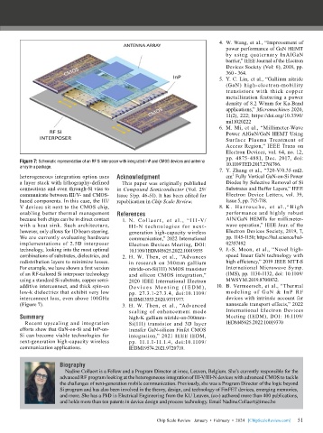
        Figure 7: Schematic representation of an RF Si interposer with integrated InP and CMOS devices and antenna   10.1109TED.2017.2761766.
        array in a package.
                                                                                7.  Y. Zhang et al., “720-V/0.35-mΩ.
                                                                                     2
        heterogeneous integration option uses   Acknowledgment                     cm  Fully Vertical GaN-on-Si Power
        a layer stack with lithography-defined   This paper was originally published   Diodes by Selective Removal of Si
        connections and even through-Si vias to   in Compound Semiconductor (Vol. 29/  Substrates and Buffer Layers,” IEEE
        communicate between III/V- and CMOS-  Issue 5/pp. 46-51). It has been edited for   Electron Device Letters, vol. 39,
        based components. In this case, the III/  republication in Chip Scale Review.  Issue 5, pp. 715-718.
        V devices sit next to the CMOS chip,                                    8.  K . H a r r o u ch e , e t  a l .,“ H ig h
        enabling better thermal management   References                            performance and highly robust
        because both chips can be in direct contact   1.  N.  C ol l a e r t ,  e t  a l .,  “ I I I -V/  AlN/GaN HEMTs for millimeter-
        with a heat sink. Such architecture,    III-N tech nologies for next-      wave operation,” IEEE Jour. of the
        however, only allows for 1D beam steering.   generation high-capacity wireless   Electron Devices Society, 2019, 7,
        We are currently evaluating hardware    communication,” 2022 International   pp. 1145-1150; https://hal.science/hal-
        implementations of 2.5D interposer      Electron Devices Meeting, DOI:     02357492
        technology, looking into the most optimal   10.1109/IEDM45625.2022.10019555  9.  J.-S. Moon, et al., “Novel high-
        combinations of substrates, dielectrics, and   2.  H. W. Then, et al., “Advances   speed linear GaN technology with
        redistribution layers to minimize losses.   in  research on  300mm gallium   high efficiency,” 2019 IEEE MTT-S
        For example, we have shown a first version   nitride-on-Si(111) NMOS transistor   International Microwave Symp.
        of an RF-tailored Si interposer technology   and silicon CMOS integration,”   (IMS), pp. 1130-1132, doi: 10.1109/
        using a standard Si substrate, copper semi-  2020 IEEE International Electron   MWSYM.2019.8700832.
        additive interconnect, and thick spin-on   D e v i c e s M e e t i n g ( I E D M ) ,   10.  B. Vermeersch, et al., “Thermal
        low-k dielectrics that exhibit very low   pp.  27.3.1-27.3.4,  doi:10.1109/  modeli ng  of  GaN  &  I n P  R F
        interconnect loss, even above 100GHz    IEDM13553.2020.9371977.            devices with intrinsic account for
        (Figure 7).                          3.  H. W. Then, et al., “Advanced     nanoscale transport effects,” 2022
                                                scaling  of  enhancement mode      International Electron Devices
        Summary                                 high-K gallium nitride-on-300mm-   Meeting (IEDM), DOI: 10.1109/
          Recent upscaling and integration      Si(111) transistor and 3D layer    IEDM45625.2022.10019370
        efforts show that GaN-on-Si and InP-on-  transfer GaN-silicon Finfet CMOS
        Si can become viable technologies for   integration,” 2021 IEEE IEDM,
        next-generation high-capacity wireless   pp. 11.1.1-11.1.4, doi:10.1109/
        communication applications.             IEDM19574.2021.9720710.


                       Biography
                         Nadine Collaert is a Fellow and a Program Director at imec, Leuven, Belgium. She’s currently responsible for the
                       advanced RF program looking at the heterogeneous integration of III-V/III-N devices with advanced CMOS to tackle
                       the challenges of next-generation mobile communication. Previously, she was a Program Director of the logic beyond
                       Si program and has also been involved in the theory, design, and technology of FinFET devices, emerging memories,
                       and more. She has a PhD in Electrical Engineering from the KU Leuven, (co-) authored more than 400 publications,
                       and holds more than ten patents in device design and process technology. Email Nadine.Collaert@imec.be


                                                                                                             51
                                                          Chip Scale Review   January  •  February  •  2024   [ChipScaleReview.com]  51

