Page 45 - ChipScale_Mar-Apr_2020-digital
P. 45
requirements in the product specification.
        The results of the analysis are used as a
        basis for design decisions to make changes
        to the LSI. Furthermore, engineers use
        this environment to compare and contrast
        completely different designs, such as
        FOWLP and FCCSP architectures.
          This closed-loop approach can be
        executed quickly, empowering engineers
        to explore a wide array of architectures.
        Engineers use these iterative analyses to
        assess costs and verification of electronic
        characteristics. With deep insight into
        the design space, engineers make optimal
        SiP decisions.
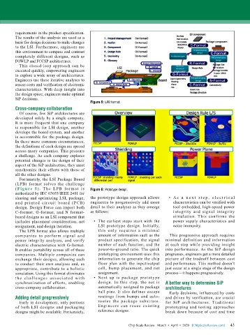
                                           Figure 5: LPB format.
        Cross-company collaboration
          Of course, few SiP architectures are
        developed solely by a single company.
        It is more frequent that one company
        is responsible for LSI design, another
        develops the board system, and another
        is accountable for the package design.
        In these more common circumstances,
        the definitions of each design are spread
        across many companies. This presents
        a challenge. As each company explores
        potential changes to the design of their
        aspect of the SiP architecture, they must
        synchronize their efforts with those of
        all the other designs.
          Fortunately, the LSI Package Board
        (LPB) format solves the challenge
        ( F i g u r e 5 ). T h e L PB fo r m a t i s   Figure 6: Prototype design.
        authorized by IEC 63055/IEEE 2401 for
        sharing and optimizing LSI, package,   the prototype design approach allows   •  A s a n ex t s t e p , e l e c t r i c a l
        and pr i nted ci rcuit board ( PCB)   engineers to progressively add more   characteristics can be verified with
        design. Design Force can import both   detail to their analyses as they emerge   tool embedded, high-speed power
        C-format, G-format, and N format-  as follows:                            integrity and signal integrity
        based designs as an LSI component that                                    simulation.  This  confirms  the
        includes placement consideration, net   •  The earliest steps start with the   power supply characteristics and
        assignment, and design iteration.      LSI prototype design. Initially,   noise immunity.
          The LPB format also allows multiple   this only requires a minimal
        companies to perfor m signal and       amount of information such as the   This progressive approach requires
        power integrity analyses, and verify   product specification, the signal   minimal definition and information
        electric characteristics with G-format.   number of each function, and the   at each step while providing insight
        It enables portability across all of these   power-to-ground ratio. The quick   into performance. As the SiP design
        companies. Multiple companies can      prototyping environment uses this   progresses, engineers get a more detailed
        exchange their designs, allowing each   information to generate the chip   picture of the tradeoff between cost
        to conduct their own analyses and, as   floor plan with the input/output   and performance. This method doesn’t
        appropriate, contribute to a holistic   cell, bump placement, and net   just occur at a single stage of the design
        simulation. Using this format eliminates   assignment.                process—it happens progressively.
        t h e  c h a l le n g e s a s s o c i a t e d w it h   •  Next up is package prototype
        synchronization of efforts, enabling   design. In this step, the net is   A better way to determine SiP
        cross-company collaboration.           automatically assigned to package   architectures
                                               ball pins. It also defines escape   Early decisions, influenced by costs
        Adding detail progressively            routings from bumps and auto-  and driven by verification, are crucial
          Early in development, only portions   routes the package substrate.   for SiP architectures. Traditional
        of both LSI designs and packaging      Engineers can reuse existing   prototyping and testing  approaches
        designs might be available. Fortunately,   reference designs.         break down because of cost and time


                                                                                                             43
                                                             Chip Scale Review   March  •  April  •  2020   [ChipScaleReview.com]  43

