Page 48 - ChipScale_Mar-Apr_2020-digital
P. 48
no longer a concern for the LAB process. The evolution of various
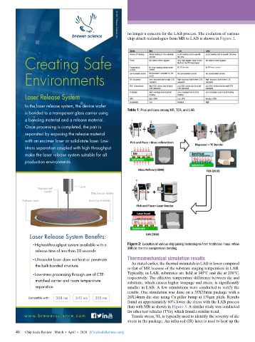
                                                           chip attach technologies from MR to LAB is shown in Figure 2.
                                                      © 2017 Brewer Science, Inc.


            Creating Safe


            Environments


            Laser Release System


            In the laser release system, the device wafer
                                                           Table 1: Pros and cons among MR, TCB, and LAB.
            is bonded to a transparent glass carrier using
            a bonding material and a release material.
            Once processing is completed, the pair is
            separated by exposing the release material
            with an excimer laser or solid-state laser. Low-
            stress separation coupled with high throughput
            make the laser release system suitable for all
            production environments.


                                     Laser
                  Transparent
                     Carrier
                                           Thin Device Wafer
           Release Layer                  Bonding Material


               Laser Release System Benefits:
                •Highest-throughput system available with a   Figure 2: Evolution of various chip joining technologies from traditional mass reflow
                 release time of less than 30 seconds       (MR) to thermal compression bonding.

                •Ultraviolet laser does not heat or penetrate   Thermomechanical simulation results
                 the bulk bonded structure                   As stated earlier, the thermal mismatch in LAB is lower compared
                                                            to that of MR because of the substrate staging temperature in LAB.
                •Low-stress processing through use of CTE-  Typically, in LAB, substrates are held at 145ºC and die at 250ºC,
                 matched carrier and room temperature       respectively. The effective temperature difference between die and
                                                            substrate, which causes higher warpage and stress, is significantly
                 separation                                 smaller in LAB. A few simulations were conducted to verify the
                                                            results. One simulation was done on a 35X35mm package with a
              Compatible with:  308 nm  343 nm  355 nm      20X14mm die size using Cu pillar bump at 130µm pitch. Results
                                                            found an approximately 60% lower die stress with the LAB process
                                                            than with MR as shown in Figure 3. A similar study was conducted
                                                            for other test vehicles (TVs), which found a similar trend.
            www.brewerscience.com                            Tensile stress, S1, is typically used to identify the severity of die
                                                            stress in the package. An infra-red (IR) laser is used to heat up the

        46
        46   Chip Scale Review   March  •  April  •  2020   [ChipScaleReview.com]

