Page 43 - ChipScale_Mar-Apr_2020-digital
P. 43
Going beyond traditional scaling with SiP


        By Yoko Fujita, Tuan Hoang  [Zuken]
        M            oore’s law  no  longer


                     r u le s  e le c t r o n i c s ’
                     m i n iat u r i zat ion [1].
        Today, companies are turning to system-
        in-package (SiP) design instead of the
        traditional f lip-chip approach. The
        drive towards SiP, however, presents
        new challenges. Engineers must assess
        perfor mance against cost factors
        early and throughout the development
        process. This article details a new
        method of gaining such insight, relying
        on simulation conducted early and
        throughout the design process, even
        merging into physical tests. As a result,
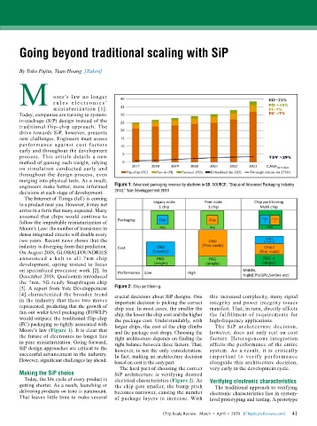
        engineers make better, more informed   Figure 1: Advanced packaging revenue by platform in $B. SOURCE: “Status of Advanced Packaging Industry
        decisions at each stage of development.  2018,” Yole Développement 2018
          The Internet of Things (IoT) is coming
        to a product near you. However, it may not
        arrive in a form that many expected. Many
        assumed that chips would continue to
        follow the improbable miniaturization of
        Moore’s Law: the number of transistors in
        dense integrated circuits will double every
        two years. Recent news shows that the
        industry is diverging from that prediction.
        On August 2018, GLOBALFOUNDRIES
        announced a halt to all 7nm chip
        development, opting instead to focus
        on specialized processor work [2]. In
        December 2018, Qualcomm introduced
        the 7nm, 5G ready Snapdragon chip
        [3]. A report from Yole Développement   Figure 2: Chip partitioning.
        [4] characterized the broader trend   crucial decisions about SiP designs. One   this increased complexity, many signal
        in the industry that these two moves   important decision is picking the correct   integrity and power integrity issues
        represented, predicting that the growth of   chip size. In most cases, the smaller the   manifest. That, in turn, directly affects
        fan-out wafer-level packaging (FOWLP)   chip, the lower the chip cost and the higher   the fulfillment of requirements for
        would outpace the traditional flip-chip   the package cost. Understandably, with   high-frequency applications.
        (FC) packaging so tightly associated with   larger chips, the cost of the chip climbs   The SiP architect u re decision,
        Moore’s law (Figure 1). It is clear that   and the package cost drops. Choosing the   however, does not only rest on cost
        the future of electronics no longer lies   right architecture depends on finding the   factors. Heterogeneous integration
        in pure miniaturization. Going forward,   right balance between these factors. That,   affects the performance of the entire
        SiP design approaches are critical to the   however, is not the only consideration.   system. As a result, it is critically
        successful advancement in the industry.   In fact, making an architecture decision   impor tant  to  ver if y  perfor mance
        However, significant challenges lay ahead.  based on cost is the easy part.  alongside this architecture decision,
                                             The hard part of choosing the correct   very early in the development cycle.
        Making the SiP choice              SiP architecture is verifying desired
          Today, the life cycle of every product is   electrical characteristics (Figure 2). As   Verifying electronic characteristics
        getting shorter. As a result, launching or   the chip gets smaller, the bump pitch   The traditional approach to verifying
        delivering products on time is paramount.   becomes narrower, causing the number   electronic characteristics lies in system-
        That leaves little time to make several   of package layers to increase. With   level prototyping and testing. A prototype


                                                                                                             41
                                                             Chip Scale Review   March  •  April  •  2020   [ChipScaleReview.com]  41

