Page 41 - ChipScale_Mar-Apr_2020-digital
P. 41
the metal stacks highlighted. Between each metal layer is a dielectric
        or low-K type of material that is stacked for device performance
        improvements. This device design has >5 microns of metal  thickness
        in total. The stack up of the layers, along with each mask step in the
        wafer fabrication facility, leads to 38 stacked layers of interfaces at
        the end of processing.
          The red areas in Figure 5 indicate examples of possible inclusions
        from dicing or potential damage that is sub-surface during dicing of
        the wafer. These sub-surface interaction points can create failures as
        they can propagate to create damage across the scribe seal into the
        active device circuitry. Blade dicing these 38 layers happens in one or
        two passes of the mechanical dicing blade. Complexities arise when
        trying to find a blade composition that is adequate to handle all the
        individual material layers and still enable a singulated part that will
        not generate a defect during operation in the final product.
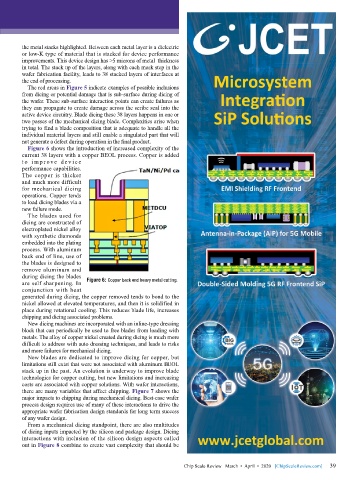
          Figure 6 shows the introduction of increased complexity of the
        current 38 layers with a copper BEOL process. Copper is added
        t o i m p r o v e  d e v i c e
        performance capabilities.
        The copper is thicker
        and much more difficult
        for mechanical dicing
        operations. Copper tends
        to load dicing blades via a
        new failure mode.
          The blades used for
        dicing are constructed of
        electroplated nickel alloy
        with synthetic diamonds
        embedded into the plating
        process. With aluminum
        back end of line, use of
        the blades is designed to
        remove aluminum and
        during dicing the blades
        are self sharpening. In   Figure 6: Copper back end heavy metal cutting.
        conjunction with heat
        generated during dicing, the copper removed tends to bond to the
        nickel allowed at elevated temperatures, and then it is solidified in
        place during rotational cooling. This reduces blade life, increases
        chipping and dicing associated problems.
          New dicing machines are incorporated with an inline-type dressing
        block that can periodically be used to free blades from loading with
        metals. The alloy of copper nickel created during dicing is much more
        difficult to address with auto dressing techniques, and leads to risks
        and more failures for mechanical dicing.
          New blades are dedicated to improve dicing for copper, but
        limitations still exist that were not associated with aluminum BEOL
        stack up in the past. An evolution is underway to improve blade
        technologies for copper cutting, but new limitations and increasing
        costs are associated with copper solutions. With wafer interactions,
        there are many variables that affect chipping. Figure 7 shows the
        major impacts to chipping during mechanical dicing. Best-case wafer
        process design requires use of many of these interactions to drive the
        appropriate wafer fabrication design standards for long term success
        of any wafer design.
          From a mechanical dicing standpoint, there are also multitudes
        of dicing inputs impacted by the silicon and package design. Dicing
        interactions with inclusion of the silicon design aspects called
        out in Figure 8 combine to create vast complexity that should be


                                                                                                             39
                                                             Chip Scale Review   March  •  April  •  2020   [ChipScaleReview.com]  39

