Page 37 - ChipScale_Mar-Apr_2020-digital
P. 37
2
        Table 2 occupies 50mm  of bonding area,   process steps that are carried out on the   applications,” MRS Proc., 970,
        which is approximately 10 times the size of   microbump die: adhesion layer deposition,   0970-Y01-04. doi:10.1557/PROC-
        the through-silicon via (TSV) area for the   seed layer deposition, lithographic process   0970-Y01-04, 2006.
        HBM2. If any one of the 31,356 links does   for pad definition, Cu electroplating, Ni   5. P. Enquist, G. Fountain, C. Petteway,
        not close, the entire chain fails the electrical   electroplating, photoresist strip, wet etch   A. Hollingsworth, H. Grady, “Low
        continuity test. The 90+% yield built in   for seed layer and adhesion layer removal.   cost of ownership scalable copper
        multiple process lots shown in Table 2   Additionally, the new method eliminates   direct bond interconnect 3D IC
        demonstrates that the DBI Ultra is capable   the underfill assembly process. The   technology for three-dimensional
        of low anneal temperature applications. We   significant process savings in wafer-level   integrated circuit applications,”
        have also demonstrated Cu-to-Cu bonding   fabrication coupled with the elimination   2009 IEEE Inter. Conf. on 3D
        after a 175ºC anneal.              of the underfill process is attractive from a   System Integ., 3DIC 2009; 1-6.
          As a means to compare the costs between   cost perspective.              10.1109/3DIC.2009.5306533.
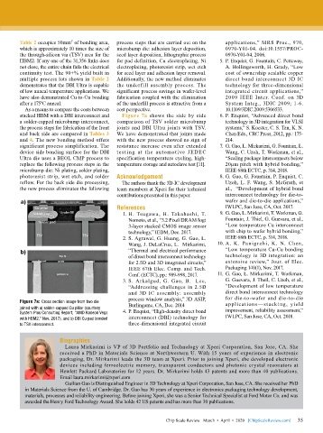
        stacked HBM with a DBI interconnect and   Figure 7a shows the side by side   6. P. Enquist, “Advanced direct bond
        a solder-capped microbump interconnect,   comparison of TSV solder microbump   technology in 3D integration for VLSI
        the process steps for fabrication of the front   joints and DBI Ultra joints with TSV.   systems,” S. Koester, C. S. Tan, K. N.
        and back side are compared in Tables 3   We have demonstrated that joints made   Chen Eds., CRC Press, 2012, pp.: 175-
        and 4. The new bonding method offers   with the new process showed no sign of   214.
        significant process simplification. The   resistance increase even after extended   7.  G. Gao, L. Mirkarimi, G. Fountain, L.
        device side bonding surface for the DBI   testing at the automotive JEDEC   Wang, C. Uzoh, T. Workman, et al.,
        Ultra die uses a BEOL CMP process to   specification temperature cycling, high-  “Scaling package interconnects below
        replace the following process steps in the   temperature storage and autoclave test [11].  20µm pitch with hybrid bonding,”
        microbump die: Ni plating, solder plating,                                 IEEE 68th ECTC, p. 314, 2018.
        photoresist strip, wet etch, and solder   Acknowledgement                8. G. Gao, G. Fountain, P. Enquist, C.
        reflow. For the back side die processing,   The authors thank the 3D-IC development   Uzoh, L. F. Wang, S. McGrath, et
        the new process eliminates the following   team members at Xperi for their technical   al.,  “Development of hybrid bond
                                           contributions presented in this paper.  interconnect technology for die-to-
                                                                                   wafer and die-to-die applications,”
                                           References                              IWLPC, San Jose, CA, Oct. 2017.
                                              1. H. Tsugawa, H. Takahashi, T.    9. G. Gao, L. Mirkarimi, T. Workman, G.
                                                Nomoto, et al., “3.2 Pixel/DRAM/logi   Fountain, J. Thiel, G. Guevara, et al.,
                                                3-layer stacked CMOS image sensor   “Low temperature Cu interconnect
                                                technology,” IEDM, Dec. 2017.      with chip to wafer hybrid bonding,”
                                              2. S. Agrawal, G. Huang, G. Gao, L.   IEEE 68th ECTC, p. 314, 2018.
                                                Wang, J. DeLaCruz, L.  Mirkarimi,   10. A. K. Panigrahi, K. N. Chen,
                                                “Thermal and electrical performance   “Low temperature Cu-Cu bonding
                                                of direct bond interconnect technology   technology in 3D integration: an
                                                for 2.5D and 3D integrated circuits,”   extensive review,” Jour. of Elec.
                                                IEEE 67th Elec. Comp. and Tech.    Packaging 140(1), Nov. 2017.
                                                Conf. (ECTC), pp.: 989-998, 2017.  11.  G. Gao, L. Mirkarimi, T. Workman,
                                              3. S. Arkalgud, G. Gao, B.  Lee,     G. Guevara, J. Theil, C. Uzoh, et al.,
                                                “Addressing challenges in 2.5D     “Development of low temperature
                                                and 3D  IC  assembly: assembly     direct bond interconnect technology
                                                process window analysis,” 3D ASIP,   for die-to-wafer and die-to-die
        Figure 7a: Cross section image from two die   Burlingame, CA, Dec. 2014    applications—stacking, yield
        joined with a) solder-capped Cu pillar (courtesy                           improvement, reliability assessment,”
        System Plus Consulting Report, “AMD Radeon Vega   4. P. Enquist, “High-density direct bond
        with HBM2,” Nov. 2017), and b) DBI Cu pad bonded   interconnect (DBI) technology for   IWLPC, San Jose, CA, Oct. 2018.
        to TSV interconnect.                    three-dimensional integrated circuit

                       Biographies
                         Laura Mirkarimi is VP of 3D Portfolio and Technology at Xperi Corporation, San Jose, CA. She
                       received a PhD in Materials Science at Northwestern U. With 15 years of experience in electronic
                       packaging, Dr. Mirkarimi leads the 3D team at Xperi. Prior to joining Xperi, she developed electronic
                       devices including ferroelectric memory, transparent conductors and photonic crystal resonators at
                       Hewlett Packard Laboratories for 12 years. Dr. Mirkarimi holds 43 patents and more than 40 publications.
                       Email laura.mirkarimi@xperi.com
                         Guilian Gao is Distinguished Engineer in 3D Technology at Xperi Corporation, San Jose, CA. She received her PhD
          in Materials Science from the U. of Cambridge. Dr. Gao has 30 years of experience in electronics packaging technology development,
          materials, processes and reliability engineering. Before joining Xperi, she was a Senior Technical Specialist at Ford Motor Co. and was
          awarded the Henry Ford Technology Award. She holds 42 US patents and has more than 30 publications.


                                                                                                             35
                                                             Chip Scale Review   March  •  April  •  2020   [ChipScaleReview.com]  35

