Page 36 - ChipScale_Mar-Apr_2020-digital
P. 36

in development. The next generation of
                                                                              bonders will push bonding pitch to the
                                                                              ultra-fine region where revolutionary 3D-
                                                                              IC integration can be enabled.

                                                                              Fine-pitch example
                                                                                Future HBM and DRAM packaging
                                                                              is expected to scale below 40µm. Our
                                                                              new bonding method can enable at
                                                                              least two generations of pitch scaling
                                                                              and the alignment accuracy can be met
                                                                              with existing high-precision flip-chip
                                                                              bonders. The two challenges addressed
                                                                              in our development are low-temperature
                                                                              anneal and multi-layer stacking. We have
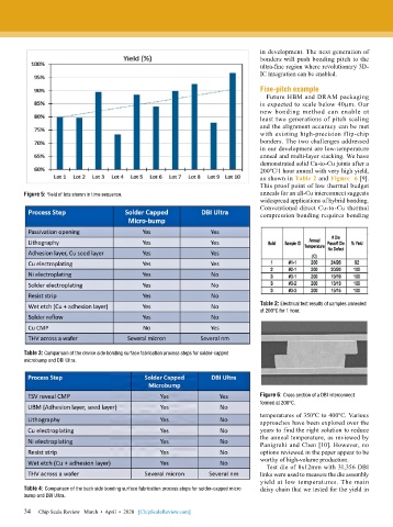
                                                                              demonstrated solid Cu-to-Cu joints after a
                                                                              200ºC/1 hour anneal with very high yield,
                                                                              as shown in Table 2 and Figure  6 [9].
                                                                              This proof point of low thermal budget
        Figure 5: Yield of lots shown in time sequence.                       anneals for an all-Cu interconnect suggests
                                                                              widespread applications of hybrid bonding.
                                                                              Conventional direct Cu-to-Cu thermal
                                                                              compression bonding requires bonding


                                                                              Table 2: Electrical test results of samples annealed
                                                                              at 200ºC for 1 hour.


        Table 3: Comparison of the device side bonding surface fabrication process steps for solder-capped
        microbump and DBI Ultra.


                                                                              Figure 6: Cross section of a DBI interconnect
                                                                              formed at 200ºC.
                                                                              temperatures of 350ºC to 400ºC. Various
                                                                              approaches have been explored over the
                                                                              years to find the right solution to reduce
                                                                              the anneal temperature, as reviewed by
                                                                              Panigrahi and Chen [10]. However, no
                                                                              options reviewed in the paper appear to be
                                                                              worthy of high-volume production.
                                                                                Test die of 8x12mm with 31,356 DBI
                                                                              links were used to measure the die assembly
                                                                              yield at low temperatures. The main
        Table 4: Comparison of the back side bonding surface fabrication process steps for solder-capped micro   daisy chain that we tested for the yield in
        bump and DBI Ultra.

        34   Chip Scale Review   March  •  April  •  2020   [ChipScaleReview.com]
        34
   31   32   33   34   35   36   37   38   39   40   41